Continue to Site

Welcome to EDAboard.com

Welcome to our site! EDAboard.com is an international Electronics Discussion Forum focused on EDA software, circuits, schematics, books, theory, papers, asic, pld, 8051, DSP, Network, RF, Analog Design, PCB, Service Manuals... and a whole lot more! To participate you need to register. Registration is free. Click here to register now.

Switching 3V3

Status
Not open for further replies.

Rajinder1268

Full Member level 3
Joined
Mar 20, 2021
Messages
162
Helped
1
Reputation
2
Reaction score
4
Trophy points
18
Activity points
1,228
Hi all,
I have an application that requires 3V3 and 5V supply.
I have two PCB's and need to switch the 3V3 to the second PCB via a connector.

What is the best way of doing this please?
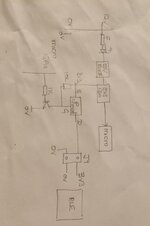
I have considered using opto MOSFET (relay), PNP transistor or p channel FET that is driven from a GPIO via a npn transistor - the p channel fet source is tied to 3V3. The gate tied to the source pin via 10K resistor i.e. keeping the p channel off. The gate is also tied to the collector of the NPN, so when this is switched on the p-channel gate is low and the device is switched. I am looking to switch 3V3 @ 500mA. I need the 3V3 to power a silicon labs BLE module.

Thanks in advance.
 

Hi,

a simple block diagram would be helpful to show how your boards are planned to be connected, as well as to see where the 3.3 V are comming from (created at board #1 ?). Also a simple circuitry would be better, than explain it by text.

I am looking to switch 3V3 @ 500mA.

Your textual explaination sounds good. Use a P-Cahnnel enhencement MOSFET with a low R_on (P_loss = 500 mA • R_on) and check its VGS threshold voltage, by means check if the MOSFET is fully turned on when VGS is -3.3 V.

BR
 

Hi,
a simple block diagram would be helpful to show how your boards are planned to be connected
I fully agree.
Without this information we can not say
* whether the MOSFET internal diode may cause problems,
* what drive voltage is available,
* whether the inrush current is too high
* ... and so on

Klaus
 

Yes , a NPN to take down the gate of a PFET sounds good..make it a logic level pfet....also, be sure to take into account the sudden inrush to the 3v3, that may take down the upstream 3v3 rail, and poss cause problems....eg reset a micro in the upstream bit...if this is the case, then you will need some inrush consideration cct aswell.......eg add a source resistor which increases vgate at the switch time...also, you can switch it on "bit by bit style"...kind of pwm it then turn it fully on...so the inrush is less
 

Hi,
I have attached a block diagram. I need some help in selecting a suitable p channel FET. I did think of in rush current but was not sure how to deal with it.
Any advice would be appreciated.
 

Attachments

  • IMG_20220501_205654.jpg
    IMG_20220501_205654.jpg
    1.9 MB · Views: 143

Hi,

please link also the BLE module you are planning to use, to check its current consumption.

A first comment regarding your block diagram, connect a shunt resistor from the base of your NPN transistor to ground (~10 k). This ensure to keep the BJT turned-off / non-conductive during powering up of your circuitry.

BR
 
Here attached are several inrush options...you can vary them as you please...its in the free LTspice simulator....you can download free.
To "see" the current in a wire....hover over the wire and go ALT + LEFTCLICK
 

Attachments

  • inrush to 3v3.zip
    2.8 KB · Views: 109
Hi,
The Bluetooth module is from Silicon Labs:
EFR32BG24
It's around 160mA when transmitting.
Thanks
--- Updated ---

Hi,

please link also the BLE module you are planning to use, to check its current consumption.

A first comment regarding your block diagram, connect a shunt resistor from the base of your NPN transistor to ground (~10 k). This ensure to keep the BJT turned-off / non-conductive during powering up of your circuitry.

BR
Will do, I totally missed this.
 

Hi,

Excuse my ignorance... Why is the NPN base resistor 1k for a 10k on the PMOS? What am I missing/not understanding?

BJT base: 3.3V - 0.7V = 2.6V
2.6V/1,000 Ohms = 2.6mA
PMOS pull-up: even the complete 3.3V/10,000 Ohms = 330uA

:unsure:

I would have expected a 10k on the NPN base (and as mentioned, an 100k or even a 1M to ground) for a 1k on the MOSFET gate pull-up; or, using the PMOS pull-up value, an 100k on the NPN base (and 1M to ground) for the 10k PMOS pull-up.

And that's a very good MOSFET with no voltage drop across the source-drain, 3.3V in = 3.3V out... ;).

Genuinely curious to know reason why for 1k base resistor. Mistake or method?
Sorry it was a mistake. I was drawing by hand as an illustration..
--- Updated ---

Sorry it was a mistake. I was drawing by hand as an illustration..
Please can you show me how you got the calculations based on the resistors. Why should I have a 100k on the NPN base (and 1M to ground) for the 10k PMOS pull-up. This is a genuine question. TIA.


Excuse my ignorance... Why is the NPN base resistor 1k for a 10k on the PMOS? What am I missing/not understanding?

BJT base: 3.3V - 0.7V = 2.6V
2.6V/1,000 Ohms = 2.6mA
PMOS pull-up: even the complete 3.3V/10,000 Ohms = 330uA

:unsure:

I would have expected a 10k on the NPN base (and as mentioned, an 100k or even a 1M to ground) for a 1k on the MOSFET gate pull-up; or, using the PMOS pull-up value, an 100k on the NPN base (and 1M to ground) for the 10k PMOS pull-up.

And that's a very good MOSFET with no voltage drop across the source-drain, 3.3V in = 3.3V out... ;).

Genuinely curious to know reason why for 1k base resistor. Mistake or method?
[/QUOTE]
--- Updated ---

Please can you show me how you got the calculations based on the resistors. Why should I have a 100k on the NPN base (and 1M to ground) for the 10k PMOS pull-up. This is a genuine question. TIA.
 
Last edited:

Hi,

Thanks for your explanation, I wouldn't apologize for a little mistake, my circuit designs are usually plagued with more perturbing mistakes than a typo ;).

As far as I remember and understand BJT resistor selection, it's typical BJT tutorial stuff, not the same as using the datasheet to select the right value based on expected hFE; it's the lazy/beginner's approach:

Presumably, we go for a BJT hFE of 10..., so if pull-up is 10k, ib should be 0.1 x ic, so Rb = 100k. If Rb is 100k, then the lazy-man's calculator says use a 1M to ground because 1M/1.1M = 0.9, and 0.9 x 2.6V (3.3V - 0.7V of the Vbe) = 2.34V means we don't lose as much of the useful/gratuitous 2.6V left over to turn the BJT on than say if we selected Rb = 100k, R pull-down = 100k, so 100k/200k = 0.5 x 2.6V = 1.3V.

Frankly, as you know, that's much of a muchness, so long as input available for Vbe is at least 0.7V (or whatever the datasheet says Vbe fully on is) and ib is around 0.1 x ic. If it were a precision circuit of some kind or the datasheet showed that hFE = 100 or 200 or whatever, I'd be more clinical about ib:ic ratio...

But I'm certain you know all this, so I'll shut up there. :)
 
Status
Not open for further replies.

Part and Inventory Search

Welcome to EDABoard.com

Sponsor

Back
Top