pforpashya
Member level 2

- Joined
- Jan 12, 2010
- Messages
- 42
- Helped
- 0
- Reputation
- 0
- Reaction score
- 0
- Trophy points
- 1,286
- Location
- जगा व जगू द्या
- Activity points
- 1,609
Hello again,
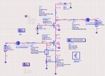
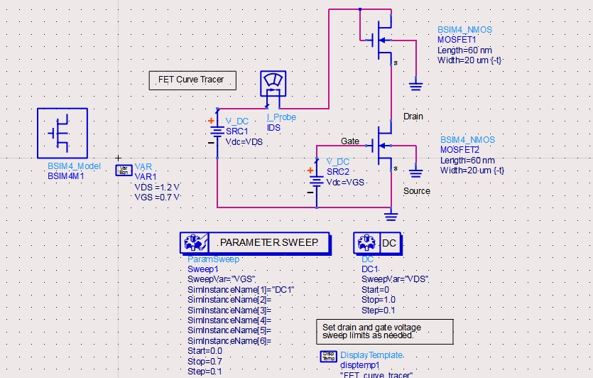
Well I have designed an mm wave amplifier(this is just first stage), as I intent to add at least two more stages and first stage being NF optimization and matching and second for gain.
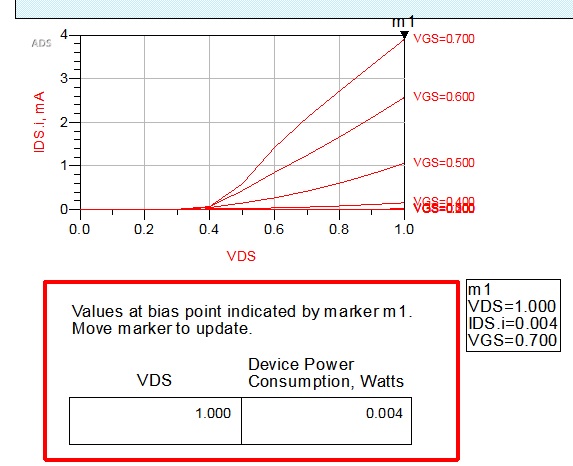
Here bias point of the amplifier is 4mA at Vds=1.2 and Vgs1=0.7v and Vgs2=1.0v with width of each transistor is 20um such that we will get Jopt=0.2mA/um
on paper to achieve above parameters we will have to have vgs-vt=0.3v and gm of 25.80mS (W/L)=333.333 L=60nm
Now the MOSFET model used is BSIM4 with all default parameters except Vt0=0.4v(Don't know how this will affect Vt as I don't know how to calculate Vt )
but assuming Vt=0.5 I given vgs of bottom mosfet as 0.7V
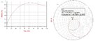
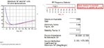
Now I am attaching the schematic as well as other result. and plz tell me what can be done to get positive gain and NF below 7dB
ps: impedance matching is not accurate I know but I guess that is not big issue
Well I have designed an mm wave amplifier(this is just first stage), as I intent to add at least two more stages and first stage being NF optimization and matching and second for gain.
Here bias point of the amplifier is 4mA at Vds=1.2 and Vgs1=0.7v and Vgs2=1.0v with width of each transistor is 20um such that we will get Jopt=0.2mA/um
on paper to achieve above parameters we will have to have vgs-vt=0.3v and gm of 25.80mS (W/L)=333.333 L=60nm
Now the MOSFET model used is BSIM4 with all default parameters except Vt0=0.4v(Don't know how this will affect Vt as I don't know how to calculate Vt )
but assuming Vt=0.5 I given vgs of bottom mosfet as 0.7V
Now I am attaching the schematic as well as other result. and plz tell me what can be done to get positive gain and NF below 7dB
ps: impedance matching is not accurate I know but I guess that is not big issue