Continue to Site

Welcome to EDAboard.com

Welcome to our site! EDAboard.com is an international Electronics Discussion Forum focused on EDA software, circuits, schematics, books, theory, papers, asic, pld, 8051, DSP, Network, RF, Analog Design, PCB, Service Manuals... and a whole lot more! To participate you need to register. Registration is free. Click here to register now.

Sudden Drain-Source Connection in Power Amplifier

Status
Not open for further replies.

darwinxie

Junior Member level 2
Joined
Dec 3, 2010
Messages
23
Helped
1
Reputation
2
Reaction score
1
Trophy points
1,283
Activity points
1,455
Hi all, I am designing a Doherty power amplifier for final project. The main amplifier is biased in class AB using NXP LDMOS BLF6G20-45 transistor.
The datasheet shows that the threshold voltage (Vth) is about 1.9 V. I biased it in 2.2V in order to go into class AB. The current at the drain is measured 0.8 A, which is far below the maximum rating (13 A). However when the power amp being tested using spectrum analyzer, a spark of fire appeared between drain and source of main amplifier.
This in turn made my transistor not working anymore (I checked it with a buzzer and the drain-source has been connected even after I disassemble the transistor) . I've wasted 2 transistors this way.
I've checked other possible short connection from bypass capacitors, bias circuit, etc. But it seems the problem only appears when the power amplifier being operated in the operating frequency (1.8 GHz).
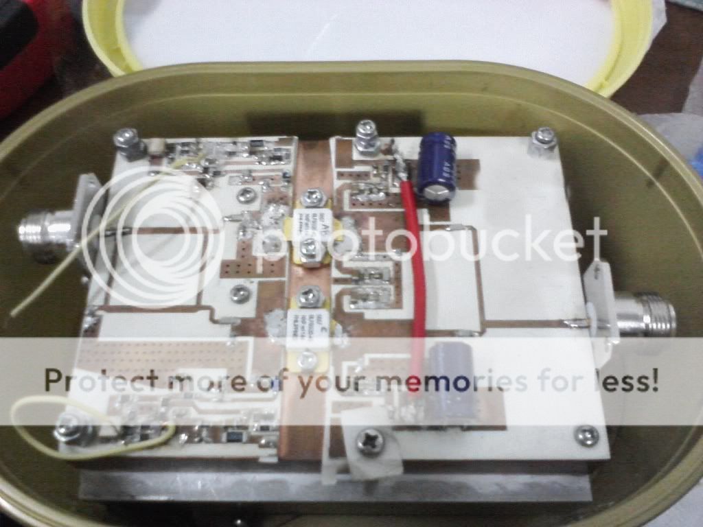
Here I attach my PCB layout. I used almost all SMD components for bias circuit, bypass, matching circuits, and snubber.
What do you think the root cause of my problem? I predict the power combiner at the output caused some signal to be reflected back to the transistors, although in ADS simulation the overall performance is satisfying enough.
I appreciate your help.
Thank you..

**broken link removed**
 
Last edited:

You neglected many other critical parameters.... eg.
- loss tangent of dielectric
- ESR of passive bypass caps at operating freq.
- size of SMD parts and their non-ideal characteristics L,C,R at 2GHz.

I suggest you are using high loss tangent PWB... useless...like putting aluminum foil in microwave oven.

you need better ($) material and get specs at 2GHz and include test coupon.
Board shops use TDR, you can use Network Analyzer. Then correlate prior to order. Ask for test coupon & test results then include coupon in your perimeter of waste area of design, then correlate.
Screen shot 2012-05-30 at 1.08.37 PM.PNG
Screen shot 2012-05-30 at 1.05.59 PM.PNG

by the way ... which university do you attend? Don't the Prof's know anything about PWB design?

What you have design, I call a dielectric plasma generator with a natural resonant frequency and negative resistance characterisic... i.e. typical for any RF mass spectrometer except they use inert gas as insulator and introduce small sample of mass burnt into gas to measure.. your dielectric is obviously not inert.. We can also call this a BBQ or a "SonofHibachi" ;p)
 

I use a Rogers 4350 PCB, so I think there is no big problem about PCB. Most of the SMD parts I use are of 0805 type in which I've included the non-ideal characteristic (stray inductance of the package).
What do you think about my design? Here I attach also the real PCB I made. The upper transistor is in class AB, the bottom one is at class C. Please give me any feedback.
Thank you.


off the top of my head....

Are the alum dielectric caps low esr? what is the SRF?
Is this microstrip with no ground plane? hmm
What about harmonic resonance?
SOA margin?
I would use polyurethane low ESR caps with high SRF caps for bypassing e.g. 30pF with solid wire with ferrite feedthru or beads from DC Vdd
Resistors are definitely a problem with 805, see link below I would expect many passives have lower SRF than you think.
**broken link removed** < consider

Board traces look at tad uneven on gaps. test it with NA to see effects of tiny solder blob.

so, 1st Assume nothing and verify passive performance with network Analyzer before reconnecting actives.. remove for now and test with NA. then test with on inserting suitable micro-coax test ports. micro coax test ports are essential for DFT.

is ground plane 1cm below just floating?

Vdd ESR may be poor from passive parts selected.. Test Vdd with Smith chart using Net Analyzer. isolated from source. Dont assume it is zero < 50µΩ

hmm no ferrite on Vdd?

More attention to passive component specs and design for testability (DFT) is suggested.Screen shot 2012-05-30 at 9.17.10 PM.PNG
 

You measure 0.8A DC Current, Not RF Current.
Power Amplifiers are generally burned because of poor load termination ( high Vds voltage or High Id current) and connection faults at input.
For instance, if you apply input signal without load with Vdd, there will be huge reflection at drain side and Vdspeak will be up to 2 times Vdd.
There might be other factors but these are very common making mistakes.
 

off the top of my head....

Are the alum dielectric caps low esr? what is the SRF?
Is this microstrip with no ground plane? hmm
What about harmonic resonance?
SOA margin?
I would use polyurethane low ESR caps with high SRF caps for bypassing e.g. 30pF with solid wire with ferrite feedthru or beads from DC Vdd
Resistors are definitely a problem with 805, see link below I would expect many passives have lower SRF than you think.
**broken link removed** < consider

Board traces look at tad uneven on gaps. test it with NA to see effects of tiny solder blob.

so, 1st Assume nothing and verify passive performance with network Analyzer before reconnecting actives.. remove for now and test with NA. then test with on inserting suitable micro-coax test ports. micro coax test ports are essential for DFT.

is ground plane 1cm below just floating?

Vdd ESR may be poor from passive parts selected.. Test Vdd with Smith chart using Net Analyzer. isolated from source. Dont assume it is zero < 50µΩ

hmm no ferrite on Vdd?

More attention to passive component specs and design for testability (DFT) is suggested.View attachment 75155


- the SRF is about 3 GHz to 4 GHz. I used Murata SMD caps, in which the datasheet claims it has low ESR value
- the ground plane is located behind the PCB (it's a double layer where the back layer acts solely as ground). The ground is also connected to copper plate and aluminium heatsink.
- I use ferrite chip 30 Ohm 0603 at the Vdd

does the mistake of passive components selection have that severe impact towards the overall performance? I'm quiet sure I have high enough SRF and voltage rating.

---------- Post added at 10:08 ---------- Previous post was at 10:03 ----------

You measure 0.8A DC Current, Not RF Current.
Power Amplifiers are generally burned because of poor load termination ( high Vds voltage or High Id current) and connection faults at input.
For instance, if you apply input signal without load with Vdd, there will be huge reflection at drain side and Vdspeak will be up to 2 times Vdd.
There might be other factors but these are very common making mistakes.

Hmm, I'm pretty sure the N connector is 50 Ohm type, towards which I design the matching network.
Do you think the power combiner cause the problem?
 

- the SRF is about 3 GHz to 4 GHz. I used Murata SMD caps, in which the datasheet claims it has low ESR value
- the ground plane is located behind the PCB (it's a double layer where the back layer acts solely as ground). The ground is also connected to copper plate and aluminium heatsink.
- I use ferrite chip 30 Ohm 0603 at the Vdd

does the mistake of passive components selection have that severe impact towards the overall performance? I'm quiet sure I have high enough SRF and voltage rating.

---------- Post added at 10:08 ---------- Previous post was at 10:03 ----------


Hmm, I'm pretty sure the N connector is 50 Ohm type, towards which I design the matching network.
Do you think the power combiner cause the problem?

Some components ( especially SMT capacitors) might be internally cracked while they are soldered.Some unseen open/short circuits can be occured.
Connectors might be poorly screwed, ground connections may be cracked,burned etc.
 

It's quite surprised to see you use a 0805 resister on the isolation port of the branch divider with these two huge transisters.

Definitely, this tiny resister won't survive after you apply high RF power in the circuit, then the input matching condition is lost. It would destroy the transistor.

Probably there are similar problems of other SMD components, especially the two coupling capacitors on the output side of the transistors. How much power they could handle.

The spark probably was due to the bias capacitors discharge when the transistor broken.

Usually the failure of the transistor is due to the oscillation, I can see the low frequency stabilization network (probably it is) in your circuit, but I can't tell the one for the in band or high frequency stabilization.

I think maybe it's better to check the stable condition.
 
Last edited:

You didn't yet talk about supply voltage. 13 A is an absolute maximum rating and hasn't to do with thermal safe operation of the device. You should always check average power supply and case temperature if possible. I presume correct transistor mounting on the heat sink.

The indicated operation mode "The upper transistor is in class AB, the bottom one is at class C" sounds problematic at first sight. Is it a verified concept (published reference design, simulation)? The transition to active operation of the class C transistor involves a change in input and output matching and operation of the combiner. The output combiner doesn't seem to provide any isolation.

I don't see from the photo, if the N-connector flange has the necessary continuation to the PCB ground plane.
 

"DC Current, Not RF Current."

I was recall an incident of fried hockey puck size power transistors that cost several hundred dollars each by a junior colleague of mine in 1975. He had a PhD and specialized in magnetics.

I was designing a micropower (50mA@12V) doppler tracking VLF 5 channel receiver, someone else the 50 watt UHF transmitter to GOES 1 and he was designing the 500W mobile windmill generator for our (world's first) mobile floating weather station.

He got scared about frying another transistor and asked me. I don't know why these pucks are failing.:shock: I have lots of voltage and current margin. "What about any RF or spurious transient power during switching" ,says I. Could this transient possibly exceed the product power for "Safe Operating Area" curve ? He said aha and then fixed his design.

It is possible to have a resonant DC supply (poor filter at one f point) from say a common gate positive feedback loop. Well only once, after that, then you think of your power supply as a transmission line with passive resonators and verify the low impedance over the maximum frequency range by some empirical test. Impulse response is one test for the stability of DC power. So I became a fan of ferrite absorption. It works even placed over DC tracks.

What I described here are rare circumstances but spurious resonances are a reality.

I agree small parts cannot handle loads, but massive SMD ceramic parts are even more brittle. I remember a major MIlitary aersopace client of ours who designed DC filters using massive ceramic with low ESR for decoupling caps on a motherboard for a turbine controller motherboard. They tended to fail under vibration testing. Thermal and mechanical stresses affected the biggest SMT ceramic caps were the worst and they could not handle any board warp and vibration in one orientation.

I agree, generally we think about power dissipation as equivalent to DC.

Also be careful not to damage small passives from hand soldering. Max temp , thermal shock , CTE concerns and solder duration must not be exceeded.

Network Analyzer tests should isolate your flaw or an RLC meter for basic failure modes. Verify your 1/4 wave shifter for return loss and look everywhere for opportunities in high reflective power.

p.s. I would have inserted a directional coupler say -20dB to monitor such conditions in the design and have diode detection of temperature or high S12 trigger a safe power limiter on DC
 
Last edited:

I believe the key to this is understanding exactly what you mean when you say " a spark of fire appeared between drain and source of main amplifier". Did you see smoke? Is there some evidence of arcing? Did some component get really hot and smoke?

My guess would be some sort of oscillation, possibly at very low frequency, took out the FETs. You might have to redesign your bias networks to quell such oscillations.
 

Did it smell like epoxy? or teflon? (both in gas states are carcinogenic I believe so be cautious) Although I knew a famous RF Tech at BRistol Aerospace Jack Askew and my mentor Bill Whitehead could tell the fried resistor value from the smell.. ;) j/k What are you using for heat sink compound? Have you tested that dielectric in a microwave oven for absorption lossy characteristics to see if it burns? ( Poor man's Network Analyzer for lossy dielectric test) e.g. 3m thermal tape vs plastic food wrap ( pre-microwave safe) and microwave safe plastic in an µwave oven will test it quickly for loss tangent. (crude but effective) It should be cold or transparent to RF.

---------- Post added at 14:22 ---------- Previous post was at 14:14 ----------

FvM yeah I was concerned about the N connector too and the sub panel ground plane being a resonant circuit. better to use smaller connectors. or improve the baseplate design to prevent a resonant cavity.

Again , a Network sweep of the critical ports should give us a better picture with S parms or Smith Chart.
 

Status
Not open for further replies.

Part and Inventory Search

Welcome to EDABoard.com

Sponsor

Back
Top