tomflo
Newbie level 5

Everyone,
I'm using the IBM cmrf8sf 130nm PDK. I've recently come upon an error I have not encountered previously and am unsure how to clear it.
From what I can tell, it stems from the NWell connection for my PMOS devices. The Calibre DRC error reads:
Check GR134: Floating (NW not over T3) found! - NWell must be tied down by M1.
I have my NWell's tied down in the same way as I have in all my previous cells - I use a large NW rectangle to surround all of the pmos devices and a cell named "nwCont" to tie the well to the metal at "vdd!". When I check previous cells that use this exact approach, I do not see the error. In addition, when I run Calibre LVS, I encounter no errors, which implies that all the NWell's are properly tied to "vdd!".
Because the foundry requires Assura DRC checks, I also run an Assura DRC, which yields 0 errors. Surprisingly, I get an error when I run Assura LVS, claiming that one of my transistors has an incorrect parameter.
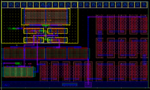
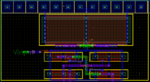
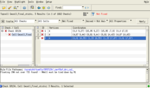
I have attached some screenshots of my layout. The first is of the full design, the second is the PMOS region, and the third is the error that appears in RVE. The coordinates that are present in RVE point to my large drawn NW region (yellow dots), the bottom left PMOS, and the nwCont NW region, respectively. I have also encountered this error in another recent design, but the layout and error is similar.
Any advice is greatly appreciated.
I'm using the IBM cmrf8sf 130nm PDK. I've recently come upon an error I have not encountered previously and am unsure how to clear it.
From what I can tell, it stems from the NWell connection for my PMOS devices. The Calibre DRC error reads:
Check GR134: Floating (NW not over T3) found! - NWell must be tied down by M1.
I have my NWell's tied down in the same way as I have in all my previous cells - I use a large NW rectangle to surround all of the pmos devices and a cell named "nwCont" to tie the well to the metal at "vdd!". When I check previous cells that use this exact approach, I do not see the error. In addition, when I run Calibre LVS, I encounter no errors, which implies that all the NWell's are properly tied to "vdd!".
Because the foundry requires Assura DRC checks, I also run an Assura DRC, which yields 0 errors. Surprisingly, I get an error when I run Assura LVS, claiming that one of my transistors has an incorrect parameter.
I have attached some screenshots of my layout. The first is of the full design, the second is the PMOS region, and the third is the error that appears in RVE. The coordinates that are present in RVE point to my large drawn NW region (yellow dots), the bottom left PMOS, and the nwCont NW region, respectively. I have also encountered this error in another recent design, but the layout and error is similar.
Any advice is greatly appreciated.