cupoftea
Advanced Member level 5
Hi,
Please comment on this method of heatsinking SMPS FETs on a FR4 PCB which lies flat in a thick aluminium heatsink?...
We have been very very briefly shown a fleeting glimpse (by Non engineers) of a 400W SMPS to be worked on, but we didn’t get much detail as we haven’t signed NDA yet. (don’t even yet know what needs doing, they said it was “flyback” and there had been a problem with the leakage inductance, and that they needed methods to get through EMC, but wouldn’t say more)
Spec is…
Vin = 24-32vdc
Vout = 30vdc
Pout = 400W
F(sw) = 250kHz (I am guessing this freq)
isolated (assume to 500vrms, 500Vdc?)
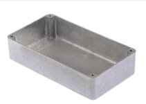
Please imagine the PCB in an Alu box (as attached). But walls approx 5 times thicker, box dims are approx. 20cm x 10cm x 5cm. It is machined from solid. The PCB lies flat in the bottom of this.
PCB was green so cant be aluminium PCB.
We saw one planar transformer in there, approx 5cm x 3.5cm x 2cm, and what looked like an SMD output inductor approx. 2.5cm x 2.5cm x1 cm. Saw a few SMD Power FETs DPAK size. All components seemed to be SMD.
Component count seemed rather low, though we suspect the bottom of the enclosure is , in places, grinded out, leaving some room for bottom side SMD components aswell.
With such a thick walled aluminium enclosure, they must be using the enclosure as a heatsink. The DPAK FETs must be thermally via’d down to the underlying aluminium base. However, that still leaves the FR4 interposing, which seems a great shame, and a wasteful diminishment of that very thick aluminium chassis for heatsinking…
1.....As such, would you agree, a better method of heatsinking the FETs would be to have TO220 FETs, layed flat, and with a cutout in the PCB, so that there tabs could be screwed down to the metal base directly?....the legs of the TO220’s would simply be snipped quite short, and they would then lay along pads next to the cutout, to which they would be soldered. This should be ok for a 1.6mm thick PCB?
2.....Also, since the chassis will inevitably be connected to circuit ground, this means there will be a significant common mode EMC problem due to the switching node of the power FETs butted up directly to the chassis. What extra EMC measures would you take in order to mitigate this?
3.....Do you also agree, chassis connection to circuit ground must be only in one place. (to avoid ground current loops and thus EMC issues)?
Please comment on this method of heatsinking SMPS FETs on a FR4 PCB which lies flat in a thick aluminium heatsink?...
We have been very very briefly shown a fleeting glimpse (by Non engineers) of a 400W SMPS to be worked on, but we didn’t get much detail as we haven’t signed NDA yet. (don’t even yet know what needs doing, they said it was “flyback” and there had been a problem with the leakage inductance, and that they needed methods to get through EMC, but wouldn’t say more)
Spec is…
Vin = 24-32vdc
Vout = 30vdc
Pout = 400W
F(sw) = 250kHz (I am guessing this freq)
isolated (assume to 500vrms, 500Vdc?)
Please imagine the PCB in an Alu box (as attached). But walls approx 5 times thicker, box dims are approx. 20cm x 10cm x 5cm. It is machined from solid. The PCB lies flat in the bottom of this.
PCB was green so cant be aluminium PCB.
We saw one planar transformer in there, approx 5cm x 3.5cm x 2cm, and what looked like an SMD output inductor approx. 2.5cm x 2.5cm x1 cm. Saw a few SMD Power FETs DPAK size. All components seemed to be SMD.
Component count seemed rather low, though we suspect the bottom of the enclosure is , in places, grinded out, leaving some room for bottom side SMD components aswell.
With such a thick walled aluminium enclosure, they must be using the enclosure as a heatsink. The DPAK FETs must be thermally via’d down to the underlying aluminium base. However, that still leaves the FR4 interposing, which seems a great shame, and a wasteful diminishment of that very thick aluminium chassis for heatsinking…
1.....As such, would you agree, a better method of heatsinking the FETs would be to have TO220 FETs, layed flat, and with a cutout in the PCB, so that there tabs could be screwed down to the metal base directly?....the legs of the TO220’s would simply be snipped quite short, and they would then lay along pads next to the cutout, to which they would be soldered. This should be ok for a 1.6mm thick PCB?
2.....Also, since the chassis will inevitably be connected to circuit ground, this means there will be a significant common mode EMC problem due to the switching node of the power FETs butted up directly to the chassis. What extra EMC measures would you take in order to mitigate this?
3.....Do you also agree, chassis connection to circuit ground must be only in one place. (to avoid ground current loops and thus EMC issues)?