Continue to Site

Welcome to EDAboard.com

Welcome to our site! EDAboard.com is an international Electronics Discussion Forum focused on EDA software, circuits, schematics, books, theory, papers, asic, pld, 8051, DSP, Network, RF, Analog Design, PCB, Service Manuals... and a whole lot more! To participate you need to register. Registration is free. Click here to register now.

[SOLVED] SMD Package Style A OPIA412ATU

Status
Not open for further replies.

nigelmercier

Member level 2
Joined
Nov 3, 2009
Messages
47
Helped
0
Reputation
0
Reaction score
0
Trophy points
1,286
Location
United Kingdom
Activity points
1,622
I have bought several OPTEK OPIA412ATU optocouplers, from the OPIA400 range. The datasheet doesn't give much in the way of soldering footprints, just that this type is "Package Style A", which may be an internal OPTEK name.

The dimensions are given thus:

SMD-A.png


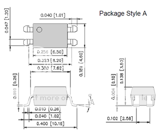
Where can I find the soldering footprint?
 

Roughly I would useas a starting point :
Four pads 1.6mm X 1.4mm (x,y).
2.58mm centre to centre Y direction to match pin spacing, 9.7mm centre to centre
X dircetion to match lead span.
 
Roughly I would useas a starting point :
Four pads 1.6mm X 1.4mm (x,y).
2.58mm centre to centre Y direction to match pin spacing, 9.7mm centre to centre
X dircetion to match lead span.

Thank you. I've had a play and come to much the same conclusion, except I made them a bit longer and spaced them at 2.54mm as I work in 1.27mm quarter grid. Having done this, I think I'm going to modify a lot more of the solder lands in my software package (DesignSpark), until now I've tended to use whatever is in the data sheet.
 

Have a look for any information relating to IPC-7351 or any wizzards, this is the defacto guide for surface mount footprints. Where possible I use IPC footprints or the wizzard to create one off footprints such as yours.yes 2.54 would do for this component as it is a PTH 2.54 pitch DIL package with the legs modified to make it a SMD device. Look out for the space between the pads across the component body, these devices are often used to isolate high voltage areas from low voltage, so often require up to 8mm isolation gap for creapage and clearance (depending on peak a.c. voltage), this can be achieved with these packages, hence they are still used for opto isolators.
 

Status
Not open for further replies.

Part and Inventory Search

Welcome to EDABoard.com

Sponsor

Back
Top