Continue to Site

Welcome to EDAboard.com

Welcome to our site! EDAboard.com is an international Electronics Discussion Forum focused on EDA software, circuits, schematics, books, theory, papers, asic, pld, 8051, DSP, Network, RF, Analog Design, PCB, Service Manuals... and a whole lot more! To participate you need to register. Registration is free. Click here to register now.

Separate ground lines for analog and digital sections

Status
Not open for further replies.

minhchau

Newbie level 6
Joined
Sep 30, 2016
Messages
14
Helped
0
Reputation
0
Reaction score
1
Trophy points
3
Location
Vietnam
Activity points
271
Hi,
My chip has the digital section and analog section, to reduce influence noise from digital, the power and ground are separated.
I can see a real effect when it comes to power separation, but separating ground doesn't seen to have much effect.
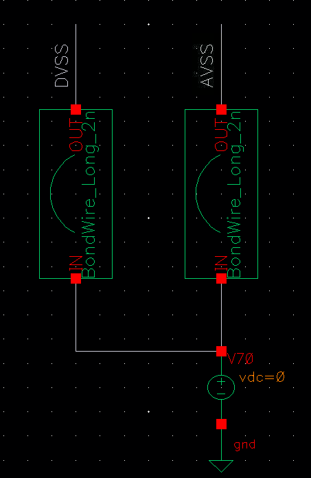
My set up DVSS and AVSS to verify separating ground showed as below:
1620453637632.png

DVSS is ground of digital section (2 bonding wire)
AVSS is ground of analog section (10 bonding wire)
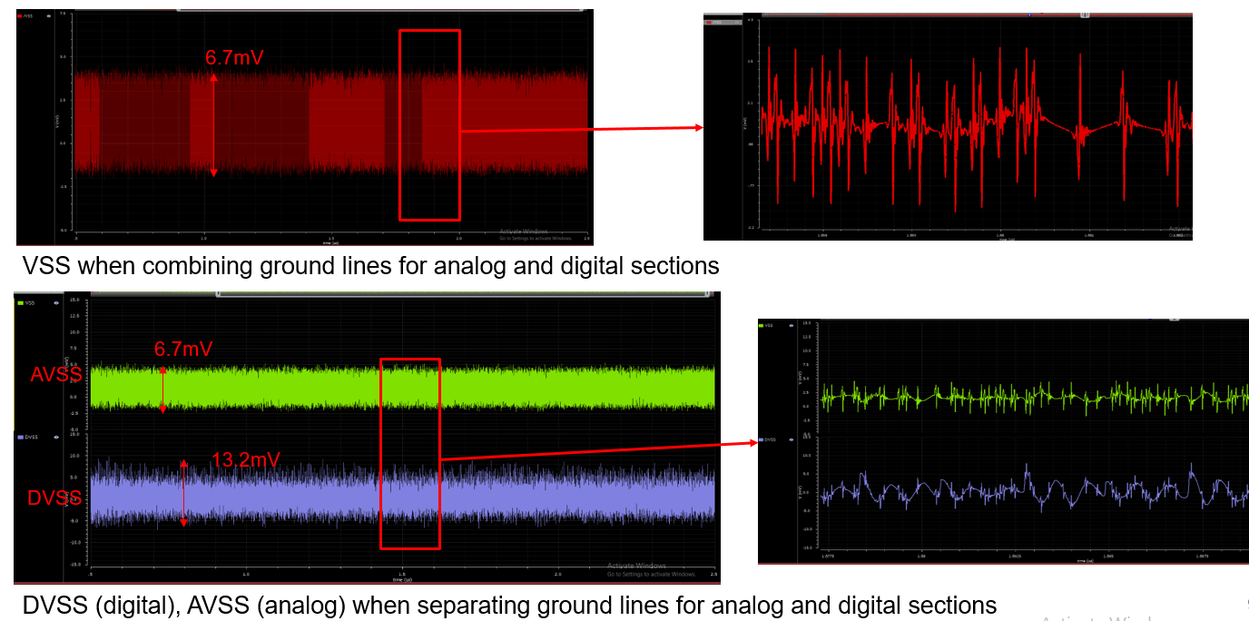
And there is simulation result:
1620453738416.png

The amplitude of AVSS is not much difference between combing and separating ground. So that, the performance does not change.

Is this result reasonable?
Are there somethin wrong with test bench?
Thanks
 

It's not clear how your "combined ground lines setup" exactly looks like. Common ground bond wires? Different ground metal layout than the separated setup?

Even more interesting, which "noise" sources do you consider? According to wave forms, you have either similar noise sources in the analog section, or other on-chip coupling pathes between digital and analog section.

Does your setup involve IO currents? Strongest effect of ground wiring is caused by ground bounce, of course only occuring with clock sources and loads connected.
Thanks FvM,
When combining ground, the ground of digital and analog will conenect together in the chip, and this ground is bonded to PCB (12 bonding wire) and when separating ground,the ground of digital and analog will seperated.

I consider the noise from digital, there is no path between digital and analog section (except bit control bus). I also find it difficult to understand why when separating the ground, the noise in AVSS doesn't change. o_O

Yes, but no clock source and loads connected
 

Status
Not open for further replies.

Part and Inventory Search

Welcome to EDABoard.com

Sponsor

Back
Top