mohamis288
Full Member level 3
Hello,
I have a question about the following self-bias circuit:
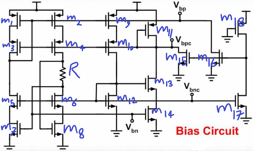
In the above circuit, m15-18 represents the start-up circuit.
How do these transistors help to start up the self-bias circuit?
what is their effect?
where does the current m15 and m16 go?
can you explain the general performance of above circuit?
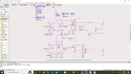
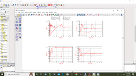
I have simulated the above circuit in ADS, and I get to the following results
( I have simulated important node voltage for different amounts of rise time for dc supply):
results without startup circuit:
results with startup circuit:
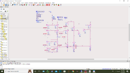
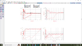
It seems there is not a significant difference between these two circuits.
I have a question about the following self-bias circuit:
In the above circuit, m15-18 represents the start-up circuit.
How do these transistors help to start up the self-bias circuit?
what is their effect?
where does the current m15 and m16 go?
can you explain the general performance of above circuit?
I have simulated the above circuit in ADS, and I get to the following results
( I have simulated important node voltage for different amounts of rise time for dc supply):
results without startup circuit:


results with startup circuit:


It seems there is not a significant difference between these two circuits.