Continue to Site

Welcome to EDAboard.com

Welcome to our site! EDAboard.com is an international Electronics Discussion Forum focused on EDA software, circuits, schematics, books, theory, papers, asic, pld, 8051, DSP, Network, RF, Analog Design, PCB, Service Manuals... and a whole lot more! To participate you need to register. Registration is free. Click here to register now.

routing strategy recommendations in ALTIUM based project

yefj

Advanced Member level 4
Joined
Sep 12, 2019
Messages
1,195
Helped
1
Reputation
2
Reaction score
3
Trophy points
38
Activity points
7,217
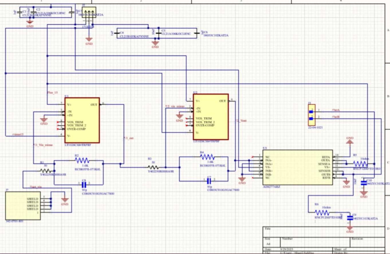
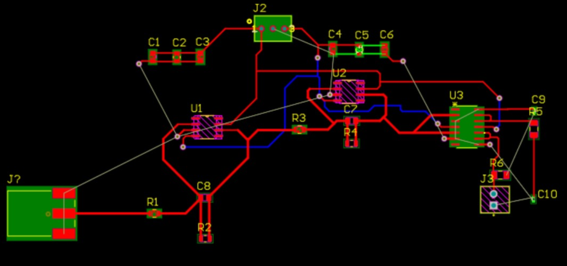
HelIo, have tried to convert my schemtics into PCB (before polygon pour). I got my traces looking very messy and its chaos. DC +15 -15 was done on the buttom layer too. I also need to do polygon pour after the traces will be ordered both on top and buttom layers ,the copper plates both will be GND net. Printscreens of my schematics and pcb shown below. My full project is attached in the link. I'll be glad to have so tip and methods on how i can improve the routing in the project.
I have few problems:
  1. my substrate is FR-4 1.6mm my connector pad width is 50 Ohm but the resistor pad is much smaller (higher impedance) i will have impedance mismatch,what should i do regarding connecting the connector with the resistor R1 ?
    2.proper routing of the V+ and V- voltage traces?
3.proper routing of the V+ and V- voltage traces?
Thanks.
https://drive.google.com/file/d/1fSMrP67edmPFymSTFb0qWmbvB33Bv6_0/view?usp=sharing
1696006594137.png

1696006619387.png
 
If you actually try impedance matched PCB design, you'll primarily care for appropriate trace width. 50 ohm microstrip on 1.6 mm FR4 is about 2.5 mm wide.

The frequency range of your circuit however doesn't require impedance matched transmission lines. A thin line acts worst case as small series inductance (e.g. some 10 nH).

The most serious problem in your PCB is lack of power supply bypass capacitors near the OPs.
 
Hello FVM ,I have put 10u 1u and 1n capcitors for decoupling as shown below, for voltage stability and noise filtering.
Also i put low pass filters at the output of the circuit as shown below.

You say i should put capacitors near the opamps.Could you please say how do i need to connect this capacitor to the +15 -15?
i thought that the decoupling capacitor at the start are doing also the filtering job.

Also if you could please reccomend me routing strategy for +15 -15 gnd track at my case.
Thanks.
1696012540787.png


1696012755922.png
 

LaTeX Commands Quick-Menu:

Part and Inventory Search

Welcome to EDABoard.com

Sponsor

Back
Top