Continue to Site

Welcome to EDAboard.com

Welcome to our site! EDAboard.com is an international Electronics Discussion Forum focused on EDA software, circuits, schematics, books, theory, papers, asic, pld, 8051, DSP, Network, RF, Analog Design, PCB, Service Manuals... and a whole lot more! To participate you need to register. Registration is free. Click here to register now.

resistor selection in inverting-noninverting amplifier

Status
Not open for further replies.

Debdut

Full Member level 3
Joined
Oct 29, 2013
Messages
174
Helped
7
Reputation
14
Reaction score
7
Trophy points
1,298
Activity points
2,572
Hello,
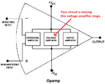
I have a two stage single output opamp. I want to create inverting and noninverting amplifiers and other circuits using the op amp.
How should the choose the resistance values that are connected at the input and feedback?
Opamp specs:
gain 75 dB
phase margin 55 degrees
unity gain bandwidth 750 MHz
slew rate 4.2 MV/s
VDD 1 V
dynamic range 0.32 - 0.7 V
current (diff. amp.) 3 uA
current (cs. amp.) 22 uA
feedback capacitor 500 fF

image002.jpg
 

Your opamp is very simple and is missing a voltage gain stage so its voltage gain will be low. Its supply voltage and operating current are extremely low. Its bandwidth and slew rate are very high for an opamp.
The resistor values must be fairly low for operation at the VHF frequencies due to stray capacitance, but the resistor values must be very high for the very low current. It looks impossible.

Here is the definition of an opamp from the internet:
 

Attachments

  • opamp.png
    opamp.png
    38.7 KB · Views: 63

As I mentioned earlier, the op amp is having 75 dB gain with power supply voltage of 1 V and its slew rate and unity gain bandwidth are as mentioned earlier.
I am not opting for high frequency operation.

Please share some information, if you have any, on resistance values to be decided for inverting and noninverting amplifier creation.
 

As I mentioned earlier, the op amp is having 75 dB gain with power supply voltage of 1 V and its slew rate and unity gain bandwidth are as mentioned earlier.
I am not opting for high frequency operation.
Please share some information, if you have any, on resistance values to be decided for inverting and noninverting amplifier creation.

There are some general rules - with the aim to treat the active unit as "ideal" as possible (during calculations):
1.) Resistors should not be too large
* because of unwanted DC voltages caused by the DC input currents (input offset)
* because they should be small against the amplifiers input resistance;
2.) Resistors should not be too small
* because they should still be large against the amplifiers output resistance
* because they must not violate the output current capability of the amplifiers output stage.
___________
As a consequence, we should try to use resistor values between 1kOhm and 100 kOhm.
 

I have never designed and built an opamp. This one has a bandwidth of 750MHz which is an ultra-high-radio-frequency and is almost microwaves. Its gain is only 75dB but most opamps have a gain of 1 Million (120dB).
Few opamps available today work from a power supply as low as 3V but this one uses only 1V!

At 750MHz a stray wiring capacitance of only 5pF has a reactance of 42 ohms which needs a lot of current to overcome.
 

current (cs. amp.) 22 uA

Now You should known the answer.

The output stage is a class A amp with 22µA biasing current. So You are not able to sink more than 22 µA its make your lower limit of resistors value.

Also, take care about any current stolen by resistor network from output amplifying device (M6) which could decrease its transconductance and result with transient stability problems.
 
  • Like
Reactions: Debdut

    Debdut

    Points: 2
    Helpful Answer Positive Rating
Hello Audioguru, the bandwidth of the op amp is low (less than MHz), I have mentioned only the unity gain bandwidth.
Also as I am creating the op amp with MOS rather than BJT, hence the gain is not large.
The process technology that I am using, provides MOSFETS with high value of Vth, I have increased the L of the MOSes to as high as possible to reduce short channel effects. And of 5 um of channel width I am experiencing Vth of nMOS to be 0.3 V. Keeping Vin = vdd/2, I only have 0.2 V as Vgs - Vth, thus current consumption is not high.

- - - Updated - - -

Thank you LvW for the information.

- - - Updated - - -

Thank you Dominik
 

Status
Not open for further replies.

Similar threads

Part and Inventory Search

Welcome to EDABoard.com

Sponsor

Back
Top