jackyzhangsh
Junior Member level 2
Hi,
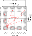
A PCB assembly factory told me that they require the relative voltage between BGA balls, which I don’t understand.
For example, for a 256-ball BGA chip:

My question is that what are they actually measuring? Does it relate to the IBIS (Input/output Buffer Information Specification) or SPICE model?
When I asked them how did they get the correct reference data for a specific chip, they told me that the data has been accumulated. For example, many of their customers used a common type of MPUs, so after they measure and solder the first such MPU from the 1st customer and had verified that the chip was good, they immediately save the measurements into an Excel file which would be stored in their database. For later customers which used the same type of MPU, they simply measure the chip and compare with their previous “known-good reference” measurements.
Does anyone know the theory behind this practice, and what is the quantity they are actually measuring? If I am their first customer using a particular chip which means they don’t have previously recorded measurement, where can I know what the “resistance” between balls are supposed to be so I can compare with the technician’s measurements to verify the “good” status of the chip? Is this information obtainable from the IC factory?
Jack
A PCB assembly factory told me that they require the relative voltage between BGA balls, which I don’t understand.
For example, for a 256-ball BGA chip:

- They would first set the multi-meter mode to “diodes”.
- Then they measures the relative “resistance” (what the technicians said, which I am not sure) between balls. Of course it doesn’t have to be done for each (ball1, ball2) pair, but would suffice if they fix one ball as a reference, and measures the “resistance” between all other balls to the reference, from which the relative “resistance” between any pair can be calculated.
- Small values can be as low as zero, and large values can be more than 300Ω, such as 310, or 400+ Ω. I am also not quite sure about whether the exact unit is Ω (ohm) here.
My question is that what are they actually measuring? Does it relate to the IBIS (Input/output Buffer Information Specification) or SPICE model?
When I asked them how did they get the correct reference data for a specific chip, they told me that the data has been accumulated. For example, many of their customers used a common type of MPUs, so after they measure and solder the first such MPU from the 1st customer and had verified that the chip was good, they immediately save the measurements into an Excel file which would be stored in their database. For later customers which used the same type of MPU, they simply measure the chip and compare with their previous “known-good reference” measurements.
Does anyone know the theory behind this practice, and what is the quantity they are actually measuring? If I am their first customer using a particular chip which means they don’t have previously recorded measurement, where can I know what the “resistance” between balls are supposed to be so I can compare with the technician’s measurements to verify the “good” status of the chip? Is this information obtainable from the IC factory?
Jack