Continue to Site

Welcome to EDAboard.com

Welcome to our site! EDAboard.com is an international Electronics Discussion Forum focused on EDA software, circuits, schematics, books, theory, papers, asic, pld, 8051, DSP, Network, RF, Analog Design, PCB, Service Manuals... and a whole lot more! To participate you need to register. Registration is free. Click here to register now.

regulated rail for inverter

Status
Not open for further replies.

hejinjie

Newbie
Joined
Aug 8, 2009
Messages
5
Helped
0
Reputation
0
Reaction score
0
Trophy points
1,281
Location
Wuxi, Jiangsu, China
Activity points
1,326
hi,

anyone got an idea to decrease the voltage of either rail of inverter output signal?
I need a 100mV~1.2V output signal and a 0V~1.12V output signal. Error within 10% @ 100mV and 1.12V.
can you help me with this design?
tinier, the better

Thanks in advance.

regards,

Kevin
 

Hi there,

I'm not sure if it could met with your specifications, but as a starting point you can try "current starved inverter". But doing it this way will increase your delay as it is actually used as a delay element.

Another way to do it is to use a H connection with common mode feedback. It is used as an LVDS transmitter mostly but even though I've not tried it myself I believe there are no objections for it to be used this way.

But please do not take my word as a reference. There should be many more topologies proposed in literature.
 

I need a 100mV~1.2V output signal and a 0V~1.12V output signal. Error within 10% @ 100mV and 1.12V.

A simple solution would be a correctly dimensioned resistor between the drain outputs of the inverter. If you could live with equal voltage drops for both directions, such a single inverter would do it. If the 2 drops have to be different (80 resp. 100mV) you'd need 2 of them.

I wonder, however, if this would work within 10% over PVT variations.
 

Connecting stabilized VSS+Offset and VDD-Offset sources seems to me the best way to achieve the intended voltage levels exactly.
 

Hi there,

I'm not sure if it could met with your specifications, but as a starting point you can try "current starved inverter". But doing it this way will increase your delay as it is actually used as a delay element.

Another way to do it is to use a H connection with common mode feedback. It is used as an LVDS transmitter mostly but even though I've not tried it myself I believe there are no objections for it to be used this way.

But please do not take my word as a reference. There should be many more topologies proposed in literature.

Thanks for reply. But it seems difficult that using a current starved inverter to meet my requirement. It relies on current and input capacitance, right?
BTW, delay is not what I am concerning about.
LVDS is actually somewhat like my design. But I am not quite familiar with that. Can you describe more details about H connection?

Thanks

---------- Post added at 10:19 ---------- Previous post was at 10:14 ----------

Connecting stabilized VSS+Offset and VDD-Offset sources seems to me the best way to achieve the intended voltage levels exactly.

It seems great. Thanks for your help. I'll see if it works. But one problem is how much does offset matter with missmatch.
 

A simple solution would be a correctly dimensioned resistor between the drain outputs of the inverter. If you could live with equal voltage drops for both directions, such a single inverter would do it. If the 2 drops have to be different (80 resp. 100mV) you'd need 2 of them.

I wonder, however, if this would work within 10% over PVT variations.

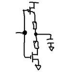
Thanks for your reply. I'm wondering if the attached figure is the structure you described.
inverter.jpg
If it is. How can I get the intended voltage?

Thanks in advance.
 

I'm wondering if the attached figure is the structure you described.
View attachment 70704
If it is. How can I get the intended voltage?

No, only one single resistor, because you want to get to the rails in one direction each:
I need a 100mV~1.2V output signal and a 0V~1.12V output signal.

And then use 2 of such inverter stages in parallel. With an output on top of the resistor (= PMOS drain) you get 100mV~1.2V.
From the other (parallel) inverter stage, from the bottom resistor connection (= NMOS drain), you can get 0V~1.12V (with correctly dimensioned resistors).
 

Status
Not open for further replies.

Part and Inventory Search

Welcome to EDABoard.com

Sponsor

Back
Top