Continue to Site

Welcome to EDAboard.com

Welcome to our site! EDAboard.com is an international Electronics Discussion Forum focused on EDA software, circuits, schematics, books, theory, papers, asic, pld, 8051, DSP, Network, RF, Analog Design, PCB, Service Manuals... and a whole lot more! To participate you need to register. Registration is free. Click here to register now.

Regulated Low Power Sine Wave

Status
Not open for further replies.

fethiyeli

Full Member level 4
Joined
Feb 9, 2013
Messages
207
Helped
10
Reputation
20
Reaction score
12
Trophy points
1,298
Activity points
2,986
Hi everyone. I need regulated 265V for testing a circuit. It needs to be between 263V and 267V and about 10W. How can i obtain regulated 265V 10W sine wave ? I know doing it with PWM method. Is there any alternative method , or which method is the best for this project ? Thnx.
 

How about an audio power amplifier and a transformer ?
Feedback from the high voltage output side should keep it pretty constant.
 
That works out to about a 7kΩ load.

Warpspeed has a good suggestion if the frequency isn't too high.
But I wouldn't try any feedback from the transformer output since the transformer high frequency phase shift will likely generate an oscillation that you will need to compensate the loop for.

What is the highest frequency you need?
 
Sorry for not mentioning about frequency. Frequency needs to be 50Hz. I have tried to implement a circuit with tda2050 and also got feedback from 265V output but i couldnt achive regulated output. I even thought adding jfet for regulation but i dont know where to add this jfet since there was no dc reference point or something in that circuit to use jfet.
 

Facing similar requirements for a low noise sin wave @5mA 200Vpeak from 0 to 100hz I went with Apex high voltage op-amps in a bridge driver topology.

You need more power than I did so you'll need larger packages and heatsinks but they have parts in exactly the territory you're talking about.

You left a lot of details out but below is an example of a bridge driver. The advantage is that you can get, say, 800 peak-to-peak from a single 400V supply which saves money on the supply and cuts power dissipation in half (and then splits it by half again between the two amplifiers). Though it may complicate your picture if you want a shared ground (because the bridge treats one amplifier as the output ground).

https://www.apexanalog.com/resources/appnotes/an03u.pdf

If this is a one-off for the lab one company that makes high voltage linear amps is Newtons 4th Lab (N4L)

- - - Updated - - -

Facing similar requirements for a low noise sin wave @5mA 200Vpeak from 0 to 100hz I went with Apex high voltage op-amps in a bridge driver topology.

You need more power than I did so you'll need larger packages and heatsinks but they have parts in exactly the territory you're talking about.

You left a lot of details out but below is an example of a bridge driver. The advantage is that you can get, say, 800 peak-to-peak from a single 400V supply which saves money on the supply and cuts power dissipation in half (and then splits it by half again between the two amplifiers). Though it may complicate your picture if you want a shared ground (because the bridge treats one amplifier as the output ground).

https://www.apexanalog.com/resources/appnotes/an03u.pdf

If this is a one-off for the lab one company that makes high voltage linear amps is Newtons 4th Lab (N4L)
 
According to post #4, the OP seems to have already a suitable power amplifier, transformer, and apparently also a generator. Problem is, he apparently doesn't know how to make a voltage controlled variable gain amplifier or attenuator.

I see many ideas when googling "JFET variable gain amplifier". There are also analog multilpliers, LDR as variable resistor, digital control with DAC...
 
Thank you all for your messages. Yeah i am using now TDA2050, 50Hz transformer with 3V (primary), 220V (secondary). I also have sine wave generator. I am getting DC voltage feedback from 265V output by rectifying it. There is a an opamp like LM358 with stable reference voltage at - input. DC voltage feedback goes through + input of LM358. JFET determines voltage divider of the input sine wave signal of TDA2050. When i loaded output about 7k resistor, output becomes about 125V from 265V. When it goes down to 125V, + input of LM358 also goes down and that makes gate - source voltage of JFET more negative. So resistance of JFET increases and input voltage of sine wave also increases. This is how i did. I am gonna put the schematic later when i finished.
 

I am supplying TDA2050 with single supply 24V and i have 3.7Vpp sine wave as input for TDA2050. I am also using TDA as inverting mode and i need to give 12VDC bias for TDA. Is there any solution to give 12V bias ? I have implemented numerous times of bias circuits i have seen on the net but none of them was successful.
 

Hi,

* I´d use a transformer 5V/230V up to 7V/230V, then you may draw more current at the 230V side. Increased overall efficiency. Maybe a toroid one.

If you don´t need isolated power, then I recommend to use the 230V signal as direct AC feedback.
Not rectifying to DC and ....

But to avoid oscillation you need the HF feedback from the TDAoutput and LF feedback from the 230V. (take care about polarity.)
I recommend to set the filter around sqrt(20000Hz x 50Hz) = 1kHz.

Then the 50Hz is feedbacked from the transformer 230V and the higher frequency is feedbacked from the amplifier output to avoid oscillations.

You may use a standard audio volume potentiometer to adjust output amplitude.


Klaus
 
162VAC - 265VAC Amplifier with JFET

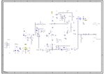
Hi everyone. I know i have already posted a topic before but now i have a schematic as shown below. I need to regulate the output at both 162VAC - 265VAC voltages. I am using JFET for regulating the output. Incoming signal is pure sine wave having 3.7Vpp. The relay is used for switching from 265VAC to 162VAC. VREF is grounded at the same time when the relay is closed. VREF is for adjusting for 162VAC. There is also a 50Hz transformer at TDA output which steps up 3.65Vrms to 265Vrms. In this JFET i use, best linear region is from about 0V to -3V as i have experimented. But now the gate voltage of JFET is always -2.6V. The problem is that it is very difficult to stabilize the system. Oscillations sometimes occur during switching no load to load or vice versa. I know its about feedback but i could not achive how to do it. Another issue is the gate voltage is always about -2.6V. Therefore switching from no load to load, there is no regulation. Even changing peak detector output, gate voltage remains same. I really need every improvements. Thnx.
162VAC - 265VAC Amplifier.jpg
 
Last edited by a moderator:

I don't see how the gate voltage can be constant -2.6V if the rectifier and control amplifier are working at all. Need to know relevant circuit node voltages to narrow down the problem.

There are unclear points in the schematic, what's the actual value of C11?
 
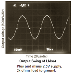
The LM324 should never be used for audio or for sine waves because it produces "crossover distortion".
 

Attachments

  • LM324 crossover distortion4.PNG
    LM324 crossover distortion4.PNG
    52.3 KB · Views: 133
LM324 isn't used as signal amplifier in the published circuit, only in the control path which should be O.K.
 
Yea i am not using LM324 for amplifying sine wave. It is used for controlling gate of the JFET. Output of the peak detector circuit which is the 3.pin of the LM324, is about 800mV or 1.1V at most when the output is 265Vrms. But when i change the reference voltage, the gate voltage remains same. The gate voltage never falls down to 0V or -500mV or something small in value. Moreover, when the peak detector output exceeds the reference voltage, output becomes very unstable. I have done this circuit before and it works pretty good but now it works very different. I have never experienced crossover distortion in this circuit. Thnx.

I used 0R resistor instead of using a capacitor there. I could use a cap there thats why i used 0R resistor. OPS components are optional and there is no component in OPS components for now. 0R resistors are used for 0R components. I did it like that since i could have placed components for improvements.
 
Last edited:

I used 0R resistor instead of using a capacitor there.
You get very low controller gain then (pure P behavior), there might be about no magnitude stabilization effect. Nevertheless you should see a gate voltage variation when adjusting the reference. Looks like some trivial circuit fault like solder short or discontinuity.

But I would go for PI controller characteristic (use C11).

Do i need the same thing in TDA feedback ? I mean the negative feedback of TDA.

Maybe i need to redesign of feedback of 4th opamp of LM324.
 
Last edited:

I think that the crossover distortion in the LM324 will cause the signal level to abruptly jump up or down a little when the DC control passes through the crossover voltage.
I think the LM324 "low power" opamp is the only opamp ever made that has crossover distortion, so why use it? There are many other cheap opamps that do not have crossover distortion.

The datasheet of the TDA2050 says that the gain must be higher than 24dB which is a gain of about 15 times, because like any analog amplifier it has frequency compensation (to prevent oscillation at a high frequency) for a certain minimum gain. It is the negative feedback that sets the amount of gain. Maybe that is causing your instability.

I see, maybe u re right because when the output voltage of the peak detector exceeds the reference voltage, system becomes unstable. There was huge amount of noises, spikes at the output of the transformer while increasing the gain in order to achieve 265V. So i added RC snubber to transformer output and all of the spikes disappeared. Moreover, sometimes increasing the voltage causes changing shape of output sinusoidal signal. I will look what i have as opamp on monday and test the circuit again.

I have not experienced any fault when the gain is lower than 24dB. Some high value of gain causes changing shape of output sinusoidal signal as i mentioned.
 

And another problem is excessive current draw from TDA. Transformer draws about 500mA from TDA output without any load at the secondary. This is maybe because of excessive magnetising current. Since i am using 220V:3V transformer as reversed so i am actually giving about 3.65Vrms to secondary in order to get about 265Vrms from primary. Maybe that causes excessive magnetising current causing more current draw from TDA output. When the output about reaches max certain level say 290V, output sinusoidal signal changes rapidly and transformer draws more current from TDA. Therefore TDA gets hot even without load and maybe i need to limit the magnetising current in order to decrease drawing current and increase efficiency.

But now i got it limiting magnetising current is not a logical solution :-D Since i may not able to get 265Vrms at output.
 
Last edited:

A simple explanation for excessive magnetizing current is that a 220V transformer isn't designed for 30% overvoltage. But you should also verify that the amplifier doesn't show parasitic high frequency oscillations.
 
Status
Not open for further replies.

Part and Inventory Search

Welcome to EDABoard.com

Sponsor

Back
Top