Continue to Site

Welcome to EDAboard.com

Welcome to our site! EDAboard.com is an international Electronics Discussion Forum focused on EDA software, circuits, schematics, books, theory, papers, asic, pld, 8051, DSP, Network, RF, Analog Design, PCB, Service Manuals... and a whole lot more! To participate you need to register. Registration is free. Click here to register now.

Reducing ringing of output voltage swing

Status
Not open for further replies.

Vijay Vinay

Member level 5
Joined
Mar 21, 2014
Messages
85
Helped
0
Reputation
0
Reaction score
0
Trophy points
6
Activity points
781
Hello all,
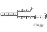
I have designed my Clock regeneration circuit in cadence Virtuoso 0.6.1. However, while I was trying to calculate the jitter of the circuitry, there was a bit overshoot and ringing in my circuitry, which I obviously needed to reduce. I need to introduce only capacitors from my bias voltage line to ground, but if I do so, there is no reduction in the ringing or overshoot. I am not sure how to solve this issue. Help is appreciated.

clock_circuitry.jpeg

ringing.jpeg
 

Attachments

  • clk_reg_circuit.jpg
    clk_reg_circuit.jpg
    49.3 KB · Views: 150

Ringing has to do with LC "tanks" and their ideality. Edge
ratesprovide the "kick" and ideality the "sustain" (cycles
of ringing, or critically or under-damped).

Some of this may be that simulations fail to include all of
the loss terms (series interconnect resistance, shunt
dielectric losses (which are a thing at RF, maybe or maybe
not at your frequencies-of-interest).

But simulations may also neglect significant "externalities"
such as wirebond inductance, cross-chip-routing inductance,
and so on which may add to the "tank set" (worth a look
as this may lead you to solve test fixturing and design for
jitter issues, early).

Adding series resistance (or undersized drivers, or putting
gate resistance in the input of the final stage) can cut
the "kick" and add lossiness. You need to position yourself
to best effect between the need for fast edges (phase
noise) and the consequence of fast edges (ringing). The
critically damped position is best I believe, although if the
ringing does not travel back over threshold of the next
stage, maybe it's only ugly without any real downside
(this has to be examined).
 

Hi dick_freebird,
I understand your point. But still my question hasn't been fully answered. Though I need inductances to increase the bandwidth of my circuitry, I couldn't eliminate them. Introducing capacitances between the Vbias and vee doesn't make any big difference. However I tried introducing Snubber circuitry internally, which had a slight change but not the whole ringing part got cancelled. So, a practical solution for my case would be the best solution in my case.
 

Status
Not open for further replies.

Part and Inventory Search

Welcome to EDABoard.com

Sponsor

Back
Top