Continue to Site

Welcome to EDAboard.com

Welcome to our site! EDAboard.com is an international Electronics Discussion Forum focused on EDA software, circuits, schematics, books, theory, papers, asic, pld, 8051, DSP, Network, RF, Analog Design, PCB, Service Manuals... and a whole lot more! To participate you need to register. Registration is free. Click here to register now.

Questions of TTL Gates ..

Status
Not open for further replies.

Mahmoud90

Newbie level 6
Joined
Feb 13, 2012
Messages
14
Helped
2
Reputation
4
Reaction score
2
Trophy points
1,283
Activity points
1,360
Excuse me, I just need answers for these questions :

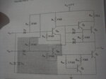
The first is : How is TTL NAND Gate modified to realize the logical AND function?
second : What is the purpose of e
ach element in the standard TTL AND gate in the fig. below ?
Attachment 71431

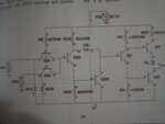
Finally .. What is the purpose of each element in the LSTTL NOR gate in the fig. below ?
Photo-0392.jpg

Thanks in advance
Photo-0394.jpg
Mahmoud​
 

Can you make the question clearer. Its hard to understand what you are trying to say.
1. You can short the IPs of NAND to get NOT gate, connect this to the OP of another NAND and you will get aa AND gate. (Or are you trying for a circuit level change?)
In the second figure, the shaded area is one of the two input sections of a basic AND gate.
 

Status
Not open for further replies.

Similar threads

Part and Inventory Search

Welcome to EDABoard.com

Sponsor

Back
Top