Continue to Site

Welcome to EDAboard.com

Welcome to our site! EDAboard.com is an international Electronics Discussion Forum focused on EDA software, circuits, schematics, books, theory, papers, asic, pld, 8051, DSP, Network, RF, Analog Design, PCB, Service Manuals... and a whole lot more! To participate you need to register. Registration is free. Click here to register now.

Questions about Amplifier Design

Status
Not open for further replies.

Xerxsea

Junior Member level 1
Joined
Jun 9, 2022
Messages
16
Helped
0
Reputation
0
Reaction score
0
Trophy points
1
Activity points
169
Hello, I've been trying to learn how transistor amplifiers work and have been trying to build one based off of a EE class assignment I found off the internet,


As per the specifications:
On the Differential Stage I set the resistors to provide 9.3v on the output and have 500uA going through the tail resistor.

I then set The Resistors in the Transistor Current Source to also fit all the specifications:
• IBIAS2 ≈ 20mA • IDIV ≈ 1.8mA (with Q5 disconnected) • VDIV ≈ 1.7V across R4

However the output of the amplifier is actually less than what goes, it attenuates the signal. I don't understand what I did wrong but my electronics knowledge is very limited so maybe I misunderstood some of the specifications that were made in determining the resistor values.

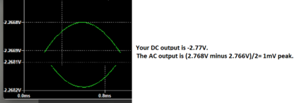
My output is -2.26v which is less than the 100mv p-p signal I started with.

Is this expected behavior and I'm misunderstanding the results? I noticed (20v-2.26v) * 0.283A (Rload Current) I get 5 Watts what is exactly what the amp should be outputting. But That -2.26v reading is in reference to ground, As is the signal generator. So that cant be.
AudioAmpCircuit.png
AudioAmp Output.png
 
Last edited:

What's up with R6 and C4? Maybe you've got other errors in your schematic as well.

And, upon further review, you've got the output connected right back to the input. I think you'd better go back and check your original source.
 

What's up with R6 and C4? Maybe you've got other errors in your schematic as well.

And, upon further review, you've got the output connected right back to the input. I think you'd better go back and check your original source.
C3,C4 and R7 and R6 were added in the final portion of the paper and the only note it has states "Impedence network comprised of R6, C2, R7, C3 provides a band-pass filter response with cutoff frequencies of approximately 16Hz and 16kHz, covering most of the audio frequency range." I did post the source, and they even included a picture of it set up on a breadboard. It seemed like it was a pretty tested solution to me but if it makes no sense then I guess not.
Edit: I just noticed what you mean with R6 and C4, In the diagram posted its shorted right through the middle. I just fixed it so that the only path is through either R6 OR C4. Removing the path in the middle. and the result is identical.
 

This is definitely not my field of expertise, but I think you’re missing a resistor in the collector of Q2. I’m pretty suspicious of this entire circuit.
 

As per the specifications:
On the Differential Stage I set the resistors to provide 9.3v on the output and have 500uA going through the tail resistor.
500 uA tail means 250 uA per transistor in balanced state. R1 dimensioned inapproriately, must be about doubled (or R2 halved). Back to stage 1 calculation.
 

Your circuit has connection errors as compared to the original, especially for the band-pass filter, so please check that.
For example, R6 and C4 appear to do nothing.

And please correct the sideways/upside-down ground connections in your schematic wiring, as they make the circuit harder to follow.
 
Last edited:

The numbers on the waveform image are so tiny and faint that they are impossible to see.
I enlarged them and increased the contrast a lot.
I seems that you measured the DC output but not the AC output.
I agree that the errors on your schematic make an attenuator, not an amplifier.
--- Updated ---

The input signal is 100mV peak, not peak-to-peak.
--- Updated ---

The input signal is 100mV peak, not peak-to-peak.
 

Attachments

  • 5W amplifier.png
    5W amplifier.png
    18.5 KB · Views: 135
Last edited:

Hi,

Ouch, ugly! Resistor as current source and resistor as current sink/tail current... Maybe try with typical two-stage OTA, that has current source and current sink around differential pair, might be easier to configure/adjust bias currents. With addition of third stage, push-pull output stage, is like UA741, etc.
 

After fixing the faults mentioned in post #2 and #5, I have no doubt that you get a functional audio amplifier, at least suited for educational purposes. Due to the class B output stage biasing, sound quality won't be mind blowing.
 
Okay, So I just got home from work, I'll Look at redoing my calculations on the first stage. but in the mean time here is the updated circuit diagram and updated output, hopefully in better resolution. Looks like I cant edit it in to the original post but here it is:
AudioAmp Output.pngAudioAmpCircuit.png

d123, I looked up a two stage OTA circuit, they seemed to be all using mosfets from what I could see. That's not a problem in itself however I was wanting to use bjts due to the fact that they confuse me a lot more than mosfets do and this was meant to be a learning experience on amplification/bjt transistors! Also I am not sure what you meant by "That has current source and current sink around differential pair"
Edit: oops that one was a 1 hz sine wave, I had been testing to see what the effect of frequency was having on the circuit, and determined that i don't think the bandpass was working properly because the output is the same as a 1khz
 
Last edited:

Feeback path corrected, input stage bias not yet. Respectively DC output offset still present.

You might post zipped LTspice file to allow others to show the correction.
 

After fixing the faults mentioned in post #2 and #5, I have no doubt that you get a functional audio amplifier, at least suited for educational purposes. Due to the class B output stage biasing, sound quality won't be mind blowing.
Okay so I have made those changes and its almost working... I am not sure how to get the ac voltage reading you guys want, when I put a cap before the load resistor the whole circuit just stops working properly and its only uV range on my output. It also now appear to be clipping off the top half, If I understand that would be due to my CE currrent Source bias voltage being too high. Is that correct?


.AudioAmpCircuit.pngAudioAmp Output.png


Here is the LTSpice schematic if anybody would like to try it out and help me improve the design!
 

Attachments

  • Audio Amp.zip
    1.3 KB · Views: 172

Also I am not sure what you meant by "That has current source and current sink around differential pair"
An ideal differential amplifier is often using current sources instead of resistors. But the project circuit isn't that bad. Suggest to correct the remaining fault and than try to improve the amplifier circuit.
--- Updated ---

Circuit is designed for DC output coupling, no need for output capacitor. Have to check why positive halfwave is clipping.
 
Last edited:
An ideal differential amplifier is often using current sources instead of resistors. But the project circuit isn't that bad. Suggest to correct the remaining fault and than try to improve the amplifier circuit.
--- Updated ---

Circuit is designed for DC output coupling, no need for output capacitor. Have to check why positive halfwave is clipping.
Okay I will try to figure out why the output is clipping. As I said, the reason I think it is clipping is the bias current/voltage on Q5 is set incorrectly, I will re do my calculations and see if I can fix it. Although that process has me very confused. I've seen online people use the Vbe Ic Graphs to find the spot with the most swing on it but i've also seen online people saying the manufacturers dont provide those graphs anymore and you never needed them to begin with.
 

Yes, your resistance of R2 is too high. But the resistor makes a lousy current source.
When you fix R2 then you get to see and hear the crossover distortion produced by having only one diode.
 

Try reducing the value of R2.
That increases the drive to Q3.
Thank you! I was barking up the wrong tree, trying to change the values of R3-5. After playing around with the value of R2 I found 510 ohms gave me a nice sine wave and the highest output and It is now definitely amplifying. Here is the output:
AudioAmp Output.png

So the peak voltage would be 1.73v - 1.057v = 0.67v. Giving me a Voltage Gain of 6.7. They say the amp is a 5 watt amplifier but I seem to be only getting about 0.67v / 8o = 0.08A * 0.67v = 0.05 peak watts? Or should I include the DC offset and use 1.73v? Which would be 0.37w per the same calculation.

How should I increase the gain? I've been trying to change the value of all the other resistors but nothing seems to increase it substantially. I removed R8 and ended up with a gain of 10, but cant seem to get any further.
 

5W into 8 ohms is an output voltage swing into 8 ohms of 17.89Vp-p.
With your input of only 200mVp-p then the gain must be 17.89/0.2= 89.45 times. But your amplifier uses 20k for R6 and 1k for R7 then its gain should be 20/1= 20 times.

An audio amplifier should be balanced so that it has NO or VERY LITTLE output offset voltage.
Your gain is so low and your output offset voltage is so high that crossover distortion is not produced.
Interesting, I did not realize R6/R7 had an effect on gain inside the passband frequency. So with the values of 20k/1k it is not possible to achieve anything over a gain of 20? How would one go about balancing the output?
 

I presume that the excercise problem can work with the specified dimensioning, particularly input stage bias of 0.5 mA, no matter if a higher bias current may be useful.

You didn't supply the Qtip31a/Qtip32a models, but there's apparently something wrong with it. I used another pair of 3A transistors from the standard LTspice library (2SCR543R/2SAR543R) and the amplifier shows +/- 8V output without distortion.

1663224161991.png
 

Attachments

  • Audio Amp.zip
    1.6 KB · Views: 122

Status
Not open for further replies.

Part and Inventory Search

Welcome to EDABoard.com

Sponsor

Back
Top