Continue to Site

Welcome to EDAboard.com

Welcome to our site! EDAboard.com is an international Electronics Discussion Forum focused on EDA software, circuits, schematics, books, theory, papers, asic, pld, 8051, DSP, Network, RF, Analog Design, PCB, Service Manuals... and a whole lot more! To participate you need to register. Registration is free. Click here to register now.

question on low drop out regulator

Status
Not open for further replies.

leonken

Full Member level 3
Joined
Jun 12, 2004
Messages
169
Helped
0
Reputation
0
Reaction score
0
Trophy points
1,296
Activity points
1,437
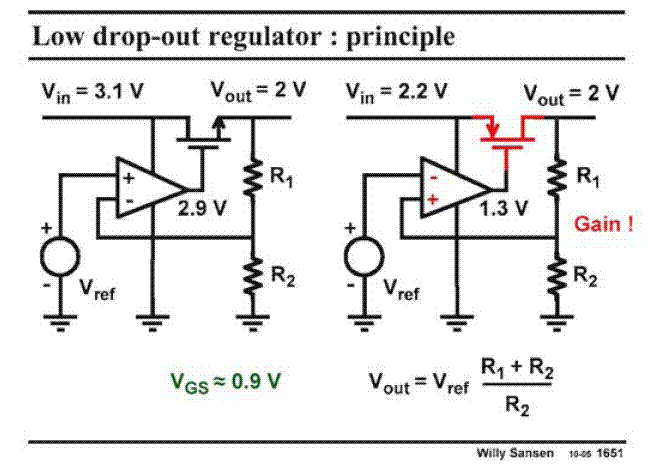
Two kind of regulators: NMOS pass device and PMOS pass device.
Why the voltage drop across the pass deivce of PMOS is smaller than the NMOS?

Added after 37 minutes:

The figure
 

voltage drop using NMOS is determined by VGS
while using PMOS it is determined by VDS
you can find the difference
 

For NMOS, Vin >VG>VS(Vout)+VTN, so VDS=Vin-Vout>VTN, but for PMOS, no such formula is expected.
 

Because the Vdd(Vin) of the opamp is supplied by Vin. The output of opamp is less than Vdd(Vin).
 

Hi,Leonken:

For NMOS , Vin is the supply of OPAMP,so Vin >VG>Vout+VTN should be met.
so VDS=Vin-Vout>VTN (about ~700mV in 0.35um process)

For PMOS,you only need to make VSD=Vin-Vout larger than Vdsat(usually about 100mV~300mV)

So the PMOS LDO headroom is larger than NMOS LDO. It is the NMOS Source follower that reduces your headroom.

Best regards!

Chenmy
 

Some LDO add a charge-pump and can also realize low drop-out with NMOS
 

because the nmos' Vgs
 

if u apply pmos pass devic the it will give u gain and phase shift of 180.
when u use nmos as pass device then it will act as a source follower.
so unity gain and no phase shift.
 

one is source follower and the other is simply common source stage
 

Status
Not open for further replies.

Part and Inventory Search

Welcome to EDABoard.com

Sponsor

Back
Top