CARFIC
Newbie level 3
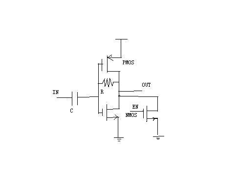
The topology of the buffer is like a basic inverter. A large capacitor is used to isolate DC in the input signal. Then the signal can be input in the inverter. In addition, a large resistor is employed to connect the input and output of the inverter. When en=0, it works normally; when en=1, it is disabled to save the power. The input signal is always VDD in disable mode. As shown in the attachment.
Now I find in diable mode, the signal after the cap is still VDD/2, so the power consumption of the buffer still has a considerable value. I tried to add more disable MOS in the possible positions, but it didn't work.
So how do I disable it to save the power consumption in disable mode? How do I place my diable transistors?
Thanks a lot.
Added after 53 minutes:
the topology of the buffer