Continue to Site

Welcome to EDAboard.com

Welcome to our site! EDAboard.com is an international Electronics Discussion Forum focused on EDA software, circuits, schematics, books, theory, papers, asic, pld, 8051, DSP, Network, RF, Analog Design, PCB, Service Manuals... and a whole lot more! To participate you need to register. Registration is free. Click here to register now.

question about switch capacitor

Status
Not open for further replies.

ronptihi

Newbie
Joined
Nov 13, 2022
Messages
3
Helped
0
Reputation
0
Reaction score
0
Trophy points
1
Activity points
32
hi
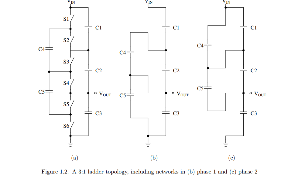
i wanted to build this circuit to try to understand him , from what i know in phase 1: vout=0.25 vin , and phase 2 :vout= 0.5 vin.
so i run transient simulation to see that my theory correct
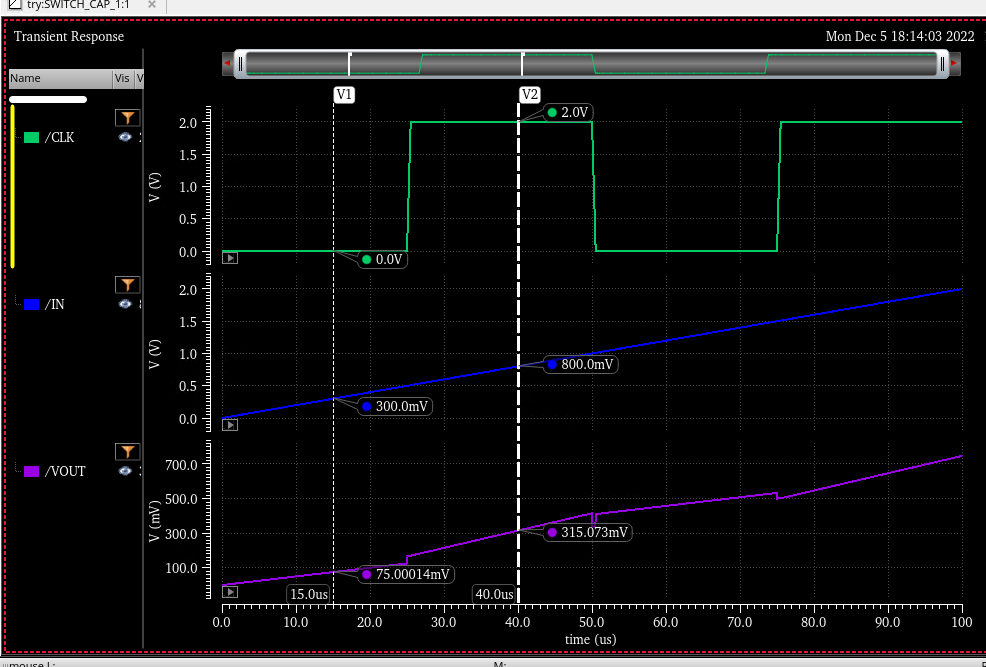
and i see in phase 1 when clk is 0 that vout is 0..25 vin
but in phase 2 when clk is VDD, vout is not 0.5 vin actually vout is 0.39 vin
why this is happen ?
sc.PNG
results.PNG
 

Switch conduction non-overlap is critical to pump efficiency.
Coincident switch "events" can allow charge leak-back during
the rise / fall time intervals. The "transfer" phase should not
start its slew until the "charge" phase has completed its', and
vice versa. The sub-schematic with all those switches stacked,
and only one clock phase shown, looks likely to suffer this.
 

ty for your answer.
i didnt understand what is it Switch conduction non-overlap is it the yellow part in the picture?
why this is happen ? and how i can prevent this ?

overlap.PNG
 

I don't understand the simulation waveforms in post #1. Why does the voltage rise continuously although the switches are only operated at the clock edges? If it's due to large Ron*C time constants, how can you expect a certain output voltage, e.g. 0.5*Vdd although the capacitors aren't charged completely?
 

the switches operate when we have VDD or GND not in clock edge
when we have GND in the CLK our schematic is on phase 1 (figure 1.2 (b) )
when we have VDD in the CLK our schematic is on phase 2 (figure 1.2 (c) ).
 

With "operate" I mean change state.

I didn't realize that Vin is ramped. Vout at t=40us can't be 0.5*Vin. Slew rate during phase2 is dVout/dt=0.5*dVin/dt. To determine the exact voltage, you need to calculate also the voltage step due to charge transfer during switch operation.
 

Status
Not open for further replies.

Part and Inventory Search

Welcome to EDABoard.com

Sponsor

Back
Top