Continue to Site

Welcome to EDAboard.com

Welcome to our site! EDAboard.com is an international Electronics Discussion Forum focused on EDA software, circuits, schematics, books, theory, papers, asic, pld, 8051, DSP, Network, RF, Analog Design, PCB, Service Manuals... and a whole lot more! To participate you need to register. Registration is free. Click here to register now.

Question about ADS EM layout: VIAGND

Status
Not open for further replies.

erihengz

Newbie
Joined
Jul 11, 2021
Messages
3
Helped
0
Reputation
0
Reaction score
1
Trophy points
3
Activity points
42
I am using VIAGND in schematic simulation. When I generate the layout from my schematic, the hole in VIAGND still visible
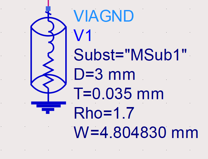
1626383320918.png

1626383118642.png


But, after converting to symbol, the hole disappear, left only the pad.
1626383155924.png

May I know if I have set the wrong layer? I have tried to connect the pin in the symbol but looks like it is open circuit. (I have set up the hole layer in the substrate editor and set the VIAGND's hole responds to the hole layer)
 

May I know if I have set the wrong layer? I have tried to connect the pin in the symbol but looks like it is open circuit. (I have set up the hole layer in the substrate editor and set the VIAGND's hole responds to the hole layer)

From your description, it is not clear where the mistake is. If you have mapped layer "hole" to the correct via layer in your Momentum stackup, you should see the short in the Momentum dataset. Check that first, to see if your Momentum model is ok.

Then, you should get the same data in schematic simulation IF you have created the emModel view properly. By default, there is no emModel and you need to enable that!

See my appnote on emModel view: muehlhaus.com/support/ads-application-notes/emmodel
 
Status
Not open for further replies.

Part and Inventory Search

Welcome to EDABoard.com

Sponsor

Back
Top