Continue to Site

Welcome to EDAboard.com

Welcome to our site! EDAboard.com is an international Electronics Discussion Forum focused on EDA software, circuits, schematics, books, theory, papers, asic, pld, 8051, DSP, Network, RF, Analog Design, PCB, Service Manuals... and a whole lot more! To participate you need to register. Registration is free. Click here to register now.

PTAT Current Source low slope

Status
Not open for further replies.

Ata_sa16

Full Member level 6
Full Member level 6
Joined
Mar 29, 2016
Messages
343
Helped
59
Reputation
118
Reaction score
58
Trophy points
28
Location
Milky Way Galaxy, 179° 56′ 39.4″
Activity points
2,221
Hi all,

I have been struggling with this PTAT current source.
It works fine but problem is, it does not have enough slope. I did a lot of tuning but I never got better than this.
Do you have any suggestions ? it can be totally different circuit. I just need a PTAT bias current source with higher slope.

ptat_bias.png

Thank your for your time.
I appreciate.
 

PTAT.JPG

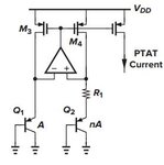
Try Implementing this topology. You can increase the slope of the PTAT current by increasing the number of parallel transistors, Q2.
Iptat=Vtln(n)/R1

- - - Updated - - -

I think that a beta current reference you've shown is inherently limited by its physical properties, i.e.
ptat beta current reference.JPG

as explained in Baker's book
 
The delta-VT generator shown could work, should not be
expected to have the same slope as a diode based ptat.
Playing with the two mirror gains (ratios) is where it's at.
Also resistor species selection, for tempco contribution.
 
View attachment 148614

Try Implementing this topology. You can increase the slope of the PTAT current by increasing the number of parallel transistors, Q2.
Iptat=Vtln(n)/R1

- - - Updated - - -

I think that a beta current reference you've shown is inherently limited by its physical properties, i.e.
View attachment 148615

as explained in Baker's book

Thank you. I will try this. Can you tell me the reference so I read about it.
And also I do not have pnp. Can I use diode connected npn ? (base is connected to collector and emitter is grounded)

- - - Updated - - -

The delta-VT generator shown could work, should not be
expected to have the same slope as a diode based ptat.
Playing with the two mirror gains (ratios) is where it's at.
Also resistor species selection, for tempco contribution.


I did a lot of tuning it does not give me better than this.

- - - Updated - - -

I got it I2 = ΔVBE / R1 and opamp is used to equalize the voltage at 2 nodes to have exactly ΔVBE on R1 (ignoring offset)
 

Can you tell me the reference so I read about it.
Design of Analog CMOS Integrated Circuits by Razavi, or CMOS Circuit Design, Layout, and Simulation 3rd ed. by Baker. They all talk about it almost the same way but I feel razavi is more intuitive while baker is more practical.

Can I use diode connected npn
Yes. I think npn is actually preferred (I'm not sure though), they only use lateral pnp because of the CMOS structure.
 

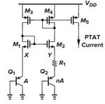
Have you tried increasing the number of parallel transistors of Q3? or tried increasing/decreasing the pmos mirror ratios? or tried using a resistor with negative tempco (some technologies have them).
Also, you can try using a different topology not using an opamp.
Capture.JPG
 

Have you tried increasing the number of parallel transistors of Q3? or tried increasing/decreasing the pmos mirror ratios? or tried using a resistor with negative tempco (some technologies have them).
Also, you can try using a different topology not using an opamp.
View attachment 148627

I tried this topology it does not give me better performance.
Do you mean Q2 ?
I tried to increase number of multipliers.
I have not tried with that type of resistor.

Thank you. I will check these points as well.
 

I am not a band-gap expert, however I have a doubt about biasing point of the circuit from #6.
In room temperature you have 132µA of current flowing to the silicon diode and the diode has 710mV (larger I suppose) and 807mV of drop. I think these values are too high, it means the point on the I-V curve is far from 0.65V drop (let's called it as "ideal" drop) for a silicon diode. Also you pmos current source are extremely inverted.

I would propose to decrease the biasing current by order of magnitude (at least, maybe even more).

The second thing, what kind of slope have you expecting?

I dont make this circuit anyway.

I want to mirror it and eventually I get

25 degrees - 6 mA
65 degrees - 7.5 mA at least
 

Hi,

I've lost my way to the wrong section, am out of my depth, and misunderstood the premise, before someone grumpy criticises me pointlessly, TIA.

I don't know if this is of any use. And sorry it's not more than a discrete concept... I'd thought maybe skipping the mirror stage and using an (in my opinion) undesirable current source might be a simpler solution, so long as a suitable buffer can be found.

Have you considered modifying a 4 to 20mA circuit for this purpose? Voltage to current conversion, using Vbe rise and amplifying it to the range needed?

Anyway, 6 to 8.3mA from 25ºC to 65ºC:

current source temp rise 25 degrees capture.JPG current source temp rise 65 degrees capture.JPG
current source temp rise schematic and graphs.JPG
 

Hi,

I've lost my way to the wrong section, am out of my depth, and misunderstood the premise, before someone grumpy criticises me pointlessly, TIA.

I don't know if this is of any use. And sorry it's not more than a discrete concept... I'd thought maybe skipping the mirror stage and using an (in my opinion) undesirable current source might be a simpler solution, so long as a suitable buffer can be found.

Have you considered modifying a 4 to 20mA circuit for this purpose? Voltage to current conversion, using Vbe rise and amplifying it to the range needed?

Anyway, 6 to 8.3mA from 25ºC to 65ºC:

View attachment 148739 View attachment 148740
View attachment 148741

Thank you for your time bro.

But this is wrong. Do you know you are doubling you power consumption with this method ?
Do you have real resistor provided by PDK ?

I cannot read your resistor values, you have 3.9 ohms ???
 

You certainly do want to be sure that the diodes are run
at a current density where they are true log-linear, or you
will be deviating from a core principle of the bandgap.
 

Hi,

Sorry that's no use for your requirements, and thanks...

Do you know you are doubling you power consumption with this method ?

Sorry, I don't understand. What do you mean?

Do you have real resistor provided by PDK ?

I had to look for what Process Design Kit is...so no. I just use the PPM setting at 100 PPM. I use a free Spice-based program (TINA TI v9) to simulate real components, I maybe mistakenly assume that such ideas can be extrapolated to IC design and the whole MOS W/L business and the heinous 20% resistors therein. I have a great fondness for voltage references and current sources/mirrors, that's why I answered your interesting thread...

I cannot read your resistor values, you have 3.9 ohms ???

That's right, 3R9 (and 71R) seem to be the magic numbers in this simulation. Paralleling three 12R could roughly re-create that value.

Your supply is 2.5V?

Hope you've found a solution.
 

Without good models for the temperature dependencies of
the diodes / FETs / BJTs and resistors your simulations are
only unvalidated fantasy.

Those resistor values would be for a "power PTAT" running
what, hundred milliamperes of bias current?

You probably can't even tell whether the device models
you are using, have a decent temperature fit or not
(add to this, whether TINA-TI treats tempco params
the same as PSPICE or whatever simulator the models
you found, are fitted for - many subtle dialect differences
between simulators).
 
  • Like
Reactions: d123

    d123

    Points: 2
    Helpful Answer Positive Rating
Can you just reduce the resistor value from the 1st schematic??
 

Status
Not open for further replies.

Part and Inventory Search

Welcome to EDABoard.com

Sponsor

Back
Top