Continue to Site

Welcome to EDAboard.com

Welcome to our site! EDAboard.com is an international Electronics Discussion Forum focused on EDA software, circuits, schematics, books, theory, papers, asic, pld, 8051, DSP, Network, RF, Analog Design, PCB, Service Manuals... and a whole lot more! To participate you need to register. Registration is free. Click here to register now.

psrr of the opamp

Status
Not open for further replies.

shanmei

Advanced Member level 1
Joined
Jul 26, 2006
Messages
430
Helped
8
Reputation
16
Reaction score
8
Trophy points
1,298
Location
USA
Activity points
4,496
This is the famous opamp architecture with good negative supply (V-) PSRR. M7 blocks the the ac signal from node A to C. There is a condition that the bias node B, the gate of M7, should be ideal, with no ac signal.

If I use a diode connection M0 bias node B. Then there is ac signal from V- will couple to B, and C, leading to a bad PSRR.

How to make bias voltage B with no ac signal?? Thanks.

paper source:
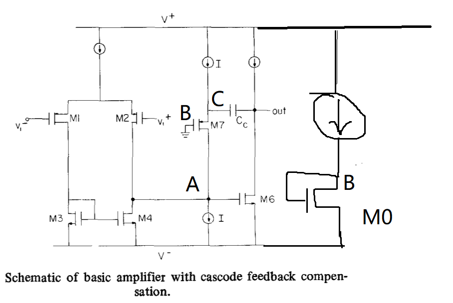


1598588113728.png
 

Hi Shanmei,

I know it's probably not the most elegant way to do that but, since you have no specs and this circuit has current source in both ways, this is the first thing I thought (please, don't make fun of me :ROFLMAO: ). In a first look, I don't think it has any headroom issue and you have high resistances from VDD and VSS.

1601338485142.png


I hope this can help you in some way.

Best regards!

Vitor
 

    shanmei

    Points: 2
    Helpful Answer Positive Rating
Thanks, Vitor.

Is this circuit from any paper?
 

Hi Shanmei,

In fact, it was just something I thought based on your question. However, I thought better and I think I have a better answer for you.

In Gray and Meyer's paper, they are considering the PSRR from V-, what makes me think that the ground there can be considered as a static reference for the whole circuit. It said, in fact this ground connection at PMOS gate does not jeopardize your negative PSRR.

In the schematic I shared, the left side of the capacitor is not well defined and mismatch between the current sources could drive some of those devices to triode region, therefore maybe is better you disregard it (sorry about that...).

What I can suggest, if the PMOS does not fit connected to ground, is a "level shift" from output's reference node (keep in mind that this output will be always "referred" do some other voltage node).

I hope this can help you.

Best regards!

Vitor
 

    shanmei

    Points: 2
    Helpful Answer Positive Rating
Thank you, Victor. Yes, ground is much cleaner.
 

Status
Not open for further replies.

Part and Inventory Search

Welcome to EDABoard.com

Sponsor

Back
Top