jimmykk
Full Member level 3
Hi all
I have designed a PCB where I am using ADG1636BRUZ SPDT Switch at +/-5V Supply Voltage to connect to my 5 piezoelectric transducers.
The motive of the design is to select one of the transducers (connected at connectors P1-P5 ) at a time and run some measurements. These piezoelectric transducers are submerged in water and can carry several hundred Volts in them.
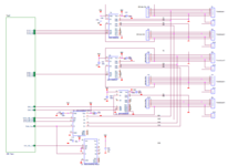
Schematics is described as follows:
3x ADG1636 Switches are used. These switches are used to connect one by one to the 5 transducers(i.e. 2 transducers with each switch). The problem with the design is that these Switches get damaged after some use which I suspect is due to the voltage coming from the transducers as there is no protection between connectors and these switches.
So, wondering if I can put any protection circuit between these ICs and connectors to save them from burning out. Would placing some protection diodes be a solution. If yes, what are the options?
I have designed a PCB where I am using ADG1636BRUZ SPDT Switch at +/-5V Supply Voltage to connect to my 5 piezoelectric transducers.
The motive of the design is to select one of the transducers (connected at connectors P1-P5 ) at a time and run some measurements. These piezoelectric transducers are submerged in water and can carry several hundred Volts in them.
Schematics is described as follows:
3x ADG1636 Switches are used. These switches are used to connect one by one to the 5 transducers(i.e. 2 transducers with each switch). The problem with the design is that these Switches get damaged after some use which I suspect is due to the voltage coming from the transducers as there is no protection between connectors and these switches.
So, wondering if I can put any protection circuit between these ICs and connectors to save them from burning out. Would placing some protection diodes be a solution. If yes, what are the options?
Last edited: