Continue to Site

Welcome to EDAboard.com

Welcome to our site! EDAboard.com is an international Electronics Discussion Forum focused on EDA software, circuits, schematics, books, theory, papers, asic, pld, 8051, DSP, Network, RF, Analog Design, PCB, Service Manuals... and a whole lot more! To participate you need to register. Registration is free. Click here to register now.

Programmable Current Sink(0mA to 1mA) with Low output voltage.

Status
Not open for further replies.

zhangz64

Junior Member level 3
Joined
May 1, 2013
Messages
25
Helped
0
Reputation
0
Reaction score
0
Trophy points
1,281
Activity points
1,632
Hi Everyone,

I am trying to design a programmable current sink with range from 0mA to 1mA.

The current sink is used to sink current from the a PMOS current mirror, therefore the voltage at output should be around 0.3V.

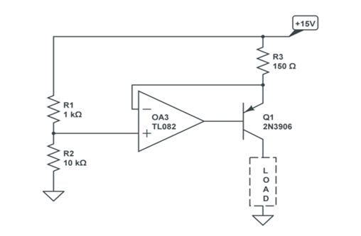
I designed the circuit with a DAC followed by a Voltage to Current convertor circuit[Adapted from a reference TI design].

The circuit worked well normally, but It does not work if the output port have a voltage lower than 1V.

I tried to tied the ground to a negative rail , but I was told that is not safe for the PMOS current mirror.

I also check the current DAC, All the current DAC i found have compliance voltage for output which is typically higher than 0.5V.
Also, Their range is hardly what i wanted.

i am kind of running out options now. I would really appreciate some input here.


So is there any way to modify my existing circuit to make it work for 0.3V output? (Attached below). [I think the reason the circuit did not work is because of the Vd of the NMOS is almost equal to the Vs of the NMOS at low output voltage. therefore no current being pushed through.]

Or if possible please suggest a better solution for this.

Thanks a lot for your help,

Best,
Eddy
Screen Shot 2016-10-13 at 5.54.33 PM.png
 

Attachments

  • Screen Shot 2016-10-13 at 5.40.06 PM.png
    Screen Shot 2016-10-13 at 5.40.06 PM.png
    68.5 KB · Views: 112
  • Screen Shot 2016-10-13 at 5.48.31 PM.png
    Screen Shot 2016-10-13 at 5.48.31 PM.png
    60.9 KB · Views: 103

A couple things, do ohms law on R2 and you'll see that it eats up 300mV at only 0.15mA. That limits you right there. Reduce it significantly so it uses no more than 100mV at your target current of 1mA (so 100 ohms).

Add a divider on the DAC accordingly so full scale on the DAC output equates to 100mV at the op-amp input pin.

Lastly I don't see any reason for the Jfet. Remove it and you can tie the output of the op-amp directly to the transistor base through a resistor.

This is another toplogy which lets your load connect directly to ground with no resistor 'using up' voltage. Though it doesn't sound like you can drive your load from the high side in this case.


[found at cdn . instructables . com/ FSQ/ H0K2/ HEXS4N45/ FSQH0K2HEXS4N45 .LARGE .jpg]
 
Last edited by a moderator:
Hi,

Thanks for the solution!

I modified the circuit as you suggested. I used a NMOS instead of those 2 transistor.
The simulation works well. I am planning to test the circuit out in lab tomorrow.
Does the circuit make sense to you?
Please let me know if you see any parts of the circuit that can be improved.

One of my concern is at the low current say 5uA.
The voltage at input of the op amp will be 1mV, Would i run into problem at this low voltage level?, etc Noise impact? should i put a cap at the input terminal?

Also, The circuit you suggested seems to be sourcing the current, That may not work for me as i am looking to sink current.

Cheers,
Eddy
Screen Shot 2016-10-13 at 8.23.24 PM.png
 

Hi,

Yes, I agree that a 100Ohms as emitter resister solves the dropout problem. (I prefer 150 ohms)

I agree that the fet/bjt combination makes it more difficult, therefore I'd simplity it.
For high accuracy I'd use amosfet instead of the combination. Maybe BSS138.
Why a mosfet? Because the bjt's base current causes current error: I_out = I_set - I_base.
The error is not big. But with a mosfet you get about zero error.

You need 150mV across 150Ohms for 1.0mA current.
If 2V DAC output should generate 1.0mA, then use a 18500:1500Ohms voltage divider.

To avoid oscillations you could use a 1500Ohms resistor to inverting input and a 10nF capacitor from opamp_output to inverting input.

Use a proper GND plane.
Select an Opamp: unity gain stable, take care about input and output voltage ranges, low noise.

Is noise an issue?

Klaus

Added:
I was a bit late.
The given circuit should work.

You could increase the capacitor values for lower noise.
Yes: opamp needs to include negative rail at common_mode_inputvoltage_range.

You could use negative supply voltage for the opamp.

Klaus
 
Hi KlausT,

Thanks for the detailed reply, Really appreciate it.

To avoid oscillations you could use a 1500Ohms resistor to inverting input and a 10nF capacitor from opamp_output to inverting input.
I believe you mean the R2 and C6 in the circuit?
What is causing the oscillation in the circuit and why would R2 and C6 reduce the oscillation?
I simulated the transiant response, it looks stable. Is there any other situation i should consider/simulate?

Also, Does it help to put a cap at Non-inverting input pin?

You could increase the capacitor values for lower noise.
Should i increase cap value for both of those caps?

Yes: opamp needs to include negative rail at common_mode_inputvoltage_range.

Is this because that The input could be as low as 1mV range, even the Op amp is rail to rail. It may not be able to output that low voltage?

Thanks,
Eddy
 

Hi,

Yes, R2, C6.
A directely feedbacked (C6) opamp may be stable, but a feedback via R3, T1, Rs1 may causees additional delay....this may cause the circuit to oscillate.

C2 reduces HF noise, because it acts like an incoming low pass filter.
C6 additionally reduces HF noise.
Increasing one or both capacitances decreases cut off frequency...reducing noise. But it slows down the regulation loop.

Negative supply rail.
An Opamp signal (input or output) is always critical when close to the supply rails.
Thus a negative supply makes it less critical.

Opa2333 should work without negative rail.

Klaus
 

Hi KlausT,

I tested the circuit in the lab today, It worked as you suggested.
I attached my measurement result here.
I measured the voltage V_in after the Voltage divider. and measured the current at Rs2(current_m). then compare with current_c = V_in/Rs1,

I have 2 additional questions:
1) I noticed there is a very consistent error above 10uA. (0.2% - 0.3%), I accounted the error at Rs1 using the measured resistance value, Also the error from voltage divider.
Where could this error coming from other than the voltage divider and Rs1?

2)I was told by someone today that I need to check the DC signal on the scope , in case "it is not bouncing around like crazy (which can happen sometimes due to unintended capacitances/inductances on the board). "

Is this the oscillation from feedback loop you are mentioning?How can i check the oscillation is not happening on scope? Should i check the NMOSE Gate and Source node voltage on the scope to make sure it is not happening?

Thanks,
Eddy


Screen Shot 2016-10-14 at 5.33.00 PM.png
Screen Shot 2016-10-14 at 4.05.04 PM.png
 

Hi,

1) are you aware you are complaining about 50nA? Even wiring or flux residuals may cause these low currents.
Regarding your percentual error calculation: you calculate the error with respect to the "estimated" value. Usually the error is calculated with respect to the "full scale". 50nA error at 1mA gives only 0.005% error.

2) oscillation. The RC feedback should avoid oscillations. If you want to measure oscillation you could measure the AC (without DC) voltage at opamp output.
Another simple verification is to compare the DC voltage of the opamp output.
When in regulation: then the output voltage must be in the range of 0.5V up to 2.5V. (Raw estimated limits)
If the opamp output voltage is outside this range, then it is very likely that the output current is not valid.

Klaus
 
Status
Not open for further replies.

Part and Inventory Search

Welcome to EDABoard.com

Sponsor

Back
Top