Continue to Site

Welcome to EDAboard.com

Welcome to our site! EDAboard.com is an international Electronics Discussion Forum focused on EDA software, circuits, schematics, books, theory, papers, asic, pld, 8051, DSP, Network, RF, Analog Design, PCB, Service Manuals... and a whole lot more! To participate you need to register. Registration is free. Click here to register now.

problem when insert clock gating

Status
Not open for further replies.

brotherjam

Newbie level 6
Joined
Dec 10, 2005
Messages
11
Helped
1
Reputation
2
Reaction score
0
Trophy points
1,281
Activity points
1,390
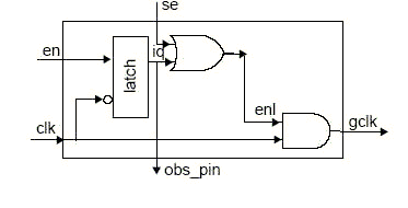
i use a integrated clock-gating cell in my design. but timing report seems to have some errors
here is the timing report.
clock gating cell TLATNTSCA.

why use clkcpu'? i think setup check should be one cycle, use clkcpu, not clkcpu':?:?:?:?:?:?

thank you very much

Startpoint: u_ts_r8051xc/U_R8051XC_U_R8051XC_CPU/cycle_reg_3_0
(rising edge-triggered flip-flop clocked by clkcpu)
Endpoint: u_ts_r8051xc/U_R8051XC_U_R8051XC_CPU/clk_gate_memaddr_s_reg/latch
(rising clock gating-check end-point clocked by clkcpu')
Path Group: **clock_gating_default**
Path Type: max

Point Incr Path

------------------------------------------------------------------------------
clock clkcpu (rise edge) 0.000 0.000
clock network delay (propagated) 1.895 1.895
u_ts_r8051xc/U_R8051XC_U_R8051XC_CPU/cycle_reg_3_0/CK (SDFFQX4)
0.000 1.895 r
u_ts_r8051xc/U_R8051XC_U_R8051XC_CPU/cycle_reg_3_0/Q (SDFFQX4)
0.373 & 2.268 r
...
u_ts_r8051xc/U_R8051XC_U_R8051XC_CPU/clk_gate_memaddr_s_reg/latch/E (TLATNTSCAX8)
4.267 & 6.536 f
data arrival time 6.536

clock clkcpu' (rise edge) 4.000 4.000
clock network delay (propagated) 1.134 5.134
clock reconvergence pessimism 0.000 5.134
u_ts_r8051xc/U_R8051XC_U_R8051XC_CPU/clk_gate_memaddr_s_reg/latch/CKcheckpin1 (TLATNTSCAX8)
5.134 r
clock gating setup time -0.223 4.911
data required time 4.911
------------------------------------------------------------------------------
data required time 4.911
data arrival time -6.536
------------------------------------------------------------------------------
slack (VIOLATED) -1.625
 

Expand the clock tree with -path full_clock_expanded and post it here.

It seems PT is checking the timing on something other than regular setup. It's been a while since I did PT last time and forgot what CKcheckpin1 was, but did you not see it in .lib ?
 

Expand the clock tree with -path full_clock_expanded and post it here.

It seems PT is checking the timing on something other than regular setup. It's been a while since I did PT last time and forgot what CKcheckpin1 was, but did you not see it in .lib ?


timing report just the same.
CKcheckpin1: see below from solvnet.
my icg is same as the figure


Question:
I modeled an integrated clock-gating "latch_posedge_postcontrol_obs" cell, as
described in the Library Compiler User Guide: Methodology and Modeling
Functionality in Technology Libraries, version 2003.03. When I compiled the
library cell, I noticed that an internal checkpin had been created and that
the timing arcs were referenced to this internal pin. However, this internal
checkpin did not exist in my original cell description.

Why is this happening and will it impact my analysis flow?
Answer:

Library Compiler creates an internal checkpin whenever a pin has a
combinational and sequential delay timing arc. This is done to separate
the two types of arcs.

The figure below shows a cell with the following two arcs:
* A positive unate combinational arc from "clk" to "gclk"
* A "falling edge" sequential arc from "clk" to "obs_pin"

9_1289641370.gif


In the figure, the setup and hold checks on "en" and the sequential delay arc
are now referenced to the internal pin "CLKcheckpin1." However, the combinational
arc is still referenced to the external pin "clk." The following report_lib_output
report shows the reference paths.

Cell Attributes # Sense/Type From To When
----------------------------------------------------------------------------
CGLPC2O b, s, u 0 pos unate CLK CLKcheckpin1
1 setup rising CLKcheckpin1 EN
2 hold rising CLKcheckpin1 EN
3 pos unate CLK GCLK
4 falling edge CLKcheckpin1 OBS_PIN

If data generated using this library information references the internal
pins, it could impact the flow if it is used with non-Synopsys tools or tools
that do not read in database-format libraries (such as simulation tools). A
typical example might be a Standard Delay Format (SDF) file created by
Design Compiler or PrimeTime.

While a Design Compiler SDF file does not reference the internal pins, a
PrimeTime file does. However, in PrimeTime version 2003.03 and earlier, you can
avoid the issue by using the -no_internal_pins option with the write_sdf
command. When you use later versions of PrimeTime, write_sdf includes an
-exclude checkpins option to help avoid the issue.
 

OK, it seems clearly explained why it's checing the timing on negedge by that article, doesn't it ? Is it not clear yet ?
 

I am sorry, but can you explain it a little? In clock gating, en just have setup&hold requirement of clk. I don't think DC has some error. So it should be my fault. How can I solve this problem?
 

if your clock gating cell is the same as the picture, you have observation output, which most probably goes to other flop or latch. That's a typical latch to latch path. Yes, it is technically one cycle path, but you usually want to make the signal setttle before the latch is open therefore it's checking the timing on the neg edge. Why ? If it couldn't meet that setup on falling edge of clock, it will cause time borrowing from the next half cycle which could make the next half cycle tighter, which you may want to avoid. That's why it checks the setup time on negedge as a precaution for potential time borrowing.

I guess if you don't have obs port, it won't check setup on checkpin, so picking the CG cell without obs might be a solution ?

Or maybe you can set multicycle path or false path to E pin of that CG cell as well as falling edge of the clock, though I haven't tried and have no idea if it works ?
 
Last edited:
problem solved

i wrote a test module yesterday, and synthesis it. report_timing, the path endpoint which is integrated clock-gating cell is reported as a "posedge clock flip-flop". I change to another target library, no timing violation. The endpoint is a "clock gating cell". I think the library isn't the same. So I read the *.lib file, compare the clock-gating cell. It seems all the same except the latter library has a attribute of "clock: true" at PIN(CK). Then I read the wrong library *.lib file with lc_shell and write to a new *.db. Use the new db file, the timing path endpoint change to "clock gating cell". It's OK now.
I think the reason is db file isnot compatible with my DC version. Regenerate the db file is a solution.

PS: Thank you, lostinxlation
 

Status
Not open for further replies.

Part and Inventory Search

Welcome to EDABoard.com

Sponsor

Back
Top