fanrong
Banned
Hi,everyone :
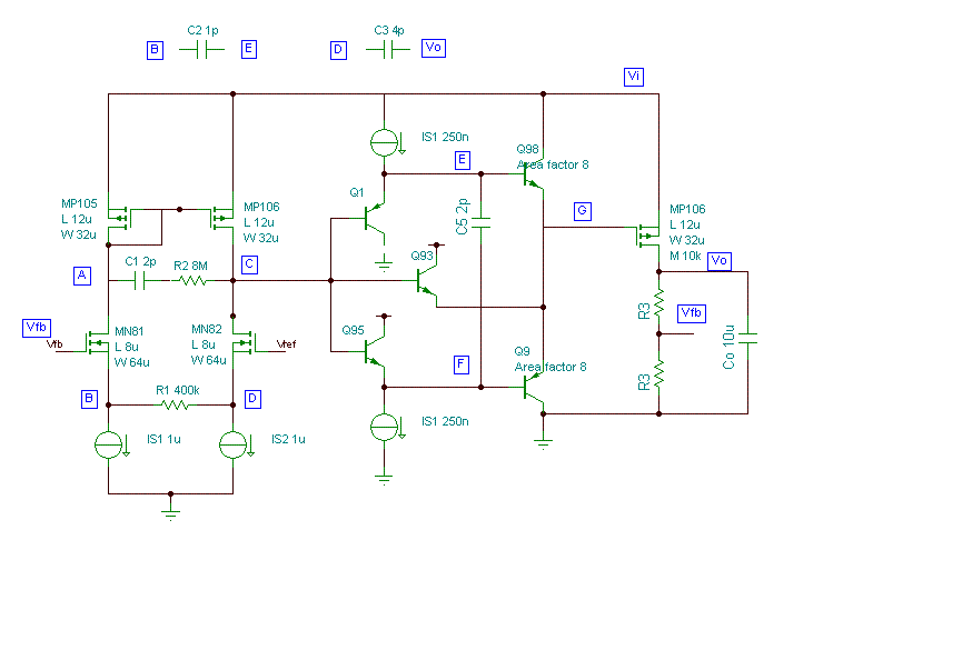
This is a LDO circuit .
R1,C2 generate a pole and a zero : p=-1/(R2+2Roc)C1 , Z=-1/R2*C1
The pole at G node : -1/2g*Cgs (1/2g=5k , Cgs=200P)
The dominate pole at the Vo : -1/Ro*Co ( Ro=50k , Co=10u)
I think C2 is to increase the speed of the loop . It may not for frequency
compensation purpose because it is connected with the source of MN81 ,which
is a low resistance node .
Initially , I think C3 is a Miller capicator for frequency purpose . But as
the Co is huge ,which is 10u ,make the gain from D node to Vo almose 0 ,even
at low frequency . So C3 is not Miller capicator , I think .
My question is :
What the function of C2 and C3 ?
https://obrazki.elektroda.pl/47_1176117535_thumb.gif
Added after 50 seconds:
https://obrazki.elektroda.pl/47_1176117535.gif
Added after 3 hours 9 minutes:

Added after 31 seconds:
url=h**p://obrazki.elektroda.pl/63_1176128926.gif
Added after 25 seconds:
h**p://obrazki.elektroda.pl/63_1176128926.gif
Added after 2 minutes:
schematic
This is a LDO circuit .
R1,C2 generate a pole and a zero : p=-1/(R2+2Roc)C1 , Z=-1/R2*C1
The pole at G node : -1/2g*Cgs (1/2g=5k , Cgs=200P)
The dominate pole at the Vo : -1/Ro*Co ( Ro=50k , Co=10u)
I think C2 is to increase the speed of the loop . It may not for frequency
compensation purpose because it is connected with the source of MN81 ,which
is a low resistance node .
Initially , I think C3 is a Miller capicator for frequency purpose . But as
the Co is huge ,which is 10u ,make the gain from D node to Vo almose 0 ,even
at low frequency . So C3 is not Miller capicator , I think .
My question is :
What the function of C2 and C3 ?
https://obrazki.elektroda.pl/47_1176117535_thumb.gif
Added after 50 seconds:
https://obrazki.elektroda.pl/47_1176117535.gif
Added after 3 hours 9 minutes:
Added after 31 seconds:
url=h**p://obrazki.elektroda.pl/63_1176128926.gif
Added after 25 seconds:
h**p://obrazki.elektroda.pl/63_1176128926.gif
Added after 2 minutes:
schematic