Continue to Site

Welcome to EDAboard.com

Welcome to our site! EDAboard.com is an international Electronics Discussion Forum focused on EDA software, circuits, schematics, books, theory, papers, asic, pld, 8051, DSP, Network, RF, Analog Design, PCB, Service Manuals... and a whole lot more! To participate you need to register. Registration is free. Click here to register now.

Pls check if latchup issue exists in this layout (Taped out)

Status
Not open for further replies.

bellona

Junior Member level 2
Joined
Apr 20, 2009
Messages
24
Helped
1
Reputation
2
Reaction score
0
Trophy points
1,281
Activity points
1,534
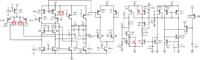
Hi, everyone. One of the op-amps in my chip isn't functioning all right. The opamp is a fully differential opamp with folded cascode PMOS input stage. The Pre and Post-simulation shows nothing wrong, it's schematic is:

I'm using a 0.35um 2p4m salicide process with non-epi substrate, VDD is 3.3V. When ever the gate voltage of the input PMOS pair (MP0 & MP1) is below 1.5V, the output of this opamp would suddenly drop to almost 0V, otherwise it would function allright, either in single to differential or inverting amplify configuration.
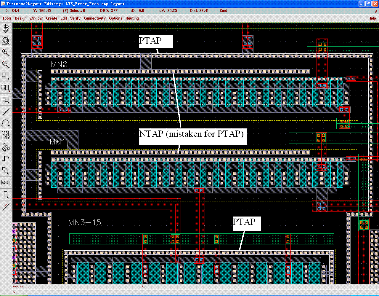
When the output drops, the current consumption of this opamp increases by about 400uA. I suspect some mild latchup might have occured which have increased the current dumping into the drain of MN3 and MN15, hence increasing the voltage at the drain of MN0 and MN1. The layout of the input differential pair is:

MP0 and MP1 is cross-coupled in 1221 fashion. NWELL1 is the n-well of MP0 and MP1, NTAP1 is the associated NTAP of these nwells, which are way too sparsely, the distance between the adjancent NTAPs in the same nwell is 40um (Design rule suggested a maximum distance of 30um). NTAP2 (built by nwell) is a nearby guardring connecting to VDD (3.3V).
Since the nwell (NWELL1) of the input transistor is not tapped right, is it possible a mild latchup might occur when the voltage of this well is lowered which dumps current into this well? Thanks in advance!
 

Could you try and perhaps simulate the effect, if you introduce additional (artificial) parasitic resistances between the S & B connections of MP0 & MP1 into your post-layout netlist? Order of 100 .. 1000 Ohms, I'd suggest.
 
  • Like
Reactions: msas

    msas

    Points: 2
    Helpful Answer Positive Rating
Re: Pls check if latchup issue exists in this layout (Taped

Hi erikl, thanks for your reply. I tried to add these backgate resistance in schematic and the result is the same. guess it's hard to simulate latchup purely from schematic?
Now i found the PTAP associated with MN0 and MN1 isn't right either. A NTAP is mistaken as PTAP during layout, as is shown this figure:

So both the NTAP for the nwell of MP0 and MP1 and the PTAP for MN0 and MN1 is not right, i guess this would increase the chance of latchup. But i couldn't figure out how this latchup works so that the voltage at the drain of MN0 and MN1 would increase? Any suggestion is highly appreciated!
 

Re: Pls check if latchup issue exists in this layout (Taped

bellona said:
Hi erikl, thanks for your reply. I tried to add these backgate resistance in schematic and the result is the same. guess it's hard to simulate latchup purely from schematic?
Hi bellona,
True; that's why I suggested to insert the resistances into the post-layout netlist!

bellona said:
Now i found the PTAP associated with MN0 and MN1 isn't right either. A NTAP is mistaken as PTAP during layout, as is shown this figure:
This creates just a useless short-circuited diode, but shouldn't do a damage. Just - again - the real (P)TAP is too far away -> increased resistance between nMOS bulk and substrate -> current-depending floating bulk potential (probably not correctly modeled by the extraction tool). Perhaps still a chance to try and simulate it by adding artificial bulk resistance in the post-layout netlist.

bellona said:
So both the NTAP for the nwell of MP0 and MP1 and the PTAP for MN0 and MN1 is not right, i guess this would increase the chance of latchup.
True. Any relatively high resistance between bulk and tap enhances the danger of latchup.

bellona said:
But i couldn't figure out how this latchup works so that the voltage at the drain of MN0 and MN1 would increase? Any suggestion is highly appreciated!
Latchup could occur (via their parasitic BJTs) between the pairs MP0/MP1 & MN3/MN15 and/or between the pairs MP5/MP6 & MN0/MN1, thereby creating a short circuit between all their sources and drains (of the affected pair). Not sure if this helps for understanding the effect.
 

    bellona

    Points: 2
    Helpful Answer Positive Rating
Short of actual latchup, operating the transistors where significant
substrate current flows could bring in the parasitic BJT and jack the
operating point around big time.

I bet there is no good model for the MOS LBJTs since the design
paradigm is for them to be well shunted at the base. So not
much chance of simulating their contribution, for which you
would also want some realistic substrate current injection
model, reasonable lateral base resistance (which is really
distributed and pinched by S/D) and so on.
 

    bellona

    Points: 2
    Helpful Answer Positive Rating
Re: Pls check if latchup issue exists in this layout (Taped

Thanks for your reply, erikl and dick_freebird.
In the process i'm using, the extractor didn't bother to extract parasitic BJTs at all. BJTs have to be labeled with a LVS_BJT layer to help extractor finding them and users are only allowed to stay with the few fixed BJT offered in PDK, like lpnp_1*1, lpnp_2*2, vpnp_1*1, vpnp_2*2 and etc. And the spice model have only modeled these fixed kind of Lateral and Vertical PNPs.
I think this really rules out the hope of simulating latchups in this process?
 

Re: Pls check if latchup issue exists in this layout (Taped

bellona said:
... the spice model have only modeled these fixed kind of Lateral and Vertical PNPs.
I think this really rules out the hope of simulating latchups in this process?
Right: Without the extraction and good models of the parasitic BJTs there's no chance.

You could, however, insert the available (modeled) BJTs (plus their respective estimated lateral base resistance = bulk-to-tap resistance) in parallel to one or both of the a.m. latchup-prone pairs and try and simulate the input voltage dependent behavior of this effect.
 

Re: Pls check if latchup issue exists in this layout (Taped

hello bellona,

first of all, the 2 transistors should be laid-out in a common-centroid manner.
please refer to the attached figure.
should there be any more problem after that, please let us know.

regards,
protonixs
 

Re: Pls check if latchup issue exists in this layout (Taped

erikl said:
You could, however, insert the available (modeled) BJTs (plus their respective estimated lateral base resistance = bulk-to-tap resistance) in parallel to one or both of the a.m. latchup-prone pairs and try and simulate the input voltage dependent behavior of this effect.
Thanks, erikl. I'll try this out and will let you know if i find some meaningful results. BTW, do you have some relevant material about manually adding those parasitic BJTs that i can reference? Thank you!

protonixs said:
hello bellona,

first of all, the 2 transistors should be laid-out in a common-centroid manner.
please refer to the attached figure.
Thanks for your reply, protonixs. The MN0 and MN1 transistors are cascode devices which doesn't affect overall matching much at low frequencies. While at high frequency their mismatch might introduce some problems like pole-zero doublets, but i think they are out of the band of interest? So i just put these two close to each other to ease the layout.
regards,
bellona
 

latch-up problem is due to intrinsic (parasitic) npnp junction, or two back-to-back BJT, also called SCR. SCR has a positive feedback and snapback I-V curve characteristics that spice model can not predict. the wrong tap connection will forward bias the PN diode junction at certain circumstances which will cause short, i think that's different from LU issue.
 

Re: Pls check if latchup issue exists in this layout (Taped

bellona said:
... do you have some relevant material about manually adding those parasitic BJTs that i can reference?
You need a vertical NPN and a lateral PNP. From fig.190-08 at the PDF below you can see their connectivity with the CMOS transistors. Use comparable areas.

The figure is from a slide of Rincón-Mora's latch-up tutorial. I've changed the original p-well on n-substrate designations at Fig. 190-08 to n-well on p-substrate (yellow rectangles - the arrows still point to the wrong direction).
Good luck!
 

Re: Pls check if latchup issue exists in this layout (Taped

prcken said:
latch-up problem is due to intrinsic (parasitic) npnp junction, or two back-to-back BJT, also called SCR. SCR has a positive feedback and snapback I-V curve characteristics that spice model can not predict. the wrong tap connection will forward bias the PN diode junction at certain circumstances which will cause short, i think that's different from LU issue.
Hi prcken, thanks for the reply. I agree with you that this might not be called latchup in this particular case, 'substrate debiasing' should be more appropriate. But i think substrate debiasing still involves current injecting into the substate, which could actually leads to latchup when this injection is beyond certain point.
erikl said:
You need a vertical NPN and a lateral PNP. From fig.190-08 at the PDF below you can see their connectivity with the CMOS transistors. Use comparable areas.

The figure is from a slide of Rincón-Mora's latch-up tutorial. I've changed the original p-well on n-substrate designations at Fig. 190-08 to n-well on p-substrate (yellow rectangles - the arrows still point to the wrong direction).
Good luck!
Thanks erikl, that's very nice of you. Guess i should try to modify some parameters like the forward current gain of my LPNP model and made up a faked NPN model, which made me pessimistic about the result.:cry:
I've fixed those substrate contact problems in the layout and i'm planning to put it as a test strcture in the second run. I'll keep this post updated.
 

Status
Not open for further replies.

Part and Inventory Search

Welcome to EDABoard.com

Sponsor

Back
Top