Continue to Site

Welcome to EDAboard.com

Welcome to our site! EDAboard.com is an international Electronics Discussion Forum focused on EDA software, circuits, schematics, books, theory, papers, asic, pld, 8051, DSP, Network, RF, Analog Design, PCB, Service Manuals... and a whole lot more! To participate you need to register. Registration is free. Click here to register now.

PLL circuit with 3 IC's

Status
Not open for further replies.

MissP.25_5

Newbie level 6
Joined
Nov 25, 2013
Messages
11
Helped
0
Reputation
0
Reaction score
0
Trophy points
1
Activity points
87
pll.JPG

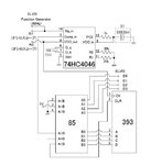
Please tell me in detail which wire should go to which number (eg. A1, B2, C4 etc...).
I am in need of big help here. I don't know what else should be done to get this correct.
I have to build this PLL circuit and choose any 3 N (integer) of the N-divider. Then I have to observe the input signal Sig_in and the output signal VCo_Out for each N. The result should be that the output frequency is N+1 times bigger than that of the frequency set by ELVIS (function generator), if I have understood the instructions correctly. I attached my results. The output signal looks weird, right? When I set N as 1, the output signal gets messed up :/ I tried for N= 4 and 8, the waveform looked just the same as when N=1. What should I do? By the way, where should I connect the 5th pin of IC 85 (A=B) to? In the diagram it just shows a short line not connecting to anything.

I took 4 pictures of different angles so you can see better. Click on the flickr links to see the pictures of my circuit. Click on the picture to zoom in.

https://www.flickr.com/photos/98820721@N04/11870437296/sizes/o/in/photostream/

https://www.flickr.com/photos/98820721@N04/11870033074/sizes/h/in/photostream/

https://www.flickr.com/photos/98820721@N04/11870445586/sizes/k/in/photostream/

https://www.flickr.com/photos/98820721@N04/11869882813/sizes/k/in/photostream/
 

Status
Not open for further replies.

Part and Inventory Search

Welcome to EDABoard.com

Sponsor

Back
Top