Continue to Site

Welcome to EDAboard.com

Welcome to our site! EDAboard.com is an international Electronics Discussion Forum focused on EDA software, circuits, schematics, books, theory, papers, asic, pld, 8051, DSP, Network, RF, Analog Design, PCB, Service Manuals... and a whole lot more! To participate you need to register. Registration is free. Click here to register now.

Please help i have fail Radiated emission in SMPS

Status
Not open for further replies.

hongtong

Newbie level 2
Joined
Feb 25, 2010
Messages
2
Helped
0
Reputation
0
Reaction score
0
Trophy points
1,281
Activity points
1,296
Hi Expert
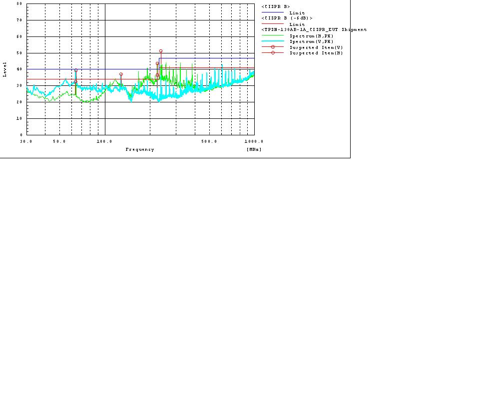
I test Radiated emission and fail on 63MHz frequency and my product is SMPS that use with printer and use flyback topology.Please advise me to improve.

Regards

92_1267075661.jpg
 

At least three factors most come together to achieve this result

- a component that generates "agressive" harmonics, most likely a schottky diode
- a resonant circuit structure, that enables 63 MHz oscillations
- unsufficiant filtering in general

It's unlikely, that 63 MHz is radiated by the board on it's own, so massive filtering of in- and output connections can be sufficient
to pass the EMI test. It's better of course, to identify the interference source. The sharp 63 MHz line indicates an unsuitable PCB
design (e.g. the commutating currents run through large area loops), it can be possibly improved by small changes.
 

Thank you FvM
Now, I use ferrite clamp on input and output wire and have change switching to slow down but result still bad.you have best solution for suggest me or not?

Regards
 

I think that at this point it would be nice to see the layout of the board. How many layers are you using on your Pcb?

-samppa
 

Have you optimized the snubber circuit component
values? These ought to minimize the "hardness" of the
switching events.

Many capacitors have poor enough ESL that they are
ineffective at 10MHz+ frequencies, if you are using a
large value cap then check its SRF and if necessary,
parallel up a couple of (say) 1nF high-Q caps to improve
the high frequency shunting.

Might try looking (say, with a 'scope) for the bad tone
on various traces, and ground, referred to the EMI test
bench ground and see where that is strongest. Using a
spectrum analyzer and a "sniffer" (couple turns of wire?)
might also let you home in, if not zero in on the source.
 

i have a similar issue with a 60 MHz spike on a isolated flyback design for a PoE converter. DC input is 48V nominal, DC output is selectable between 10V and 20V, and power is 13W. The switch frequency is 160kHz. Any ideas on where this spike could originate within a standard SMPS flyback design at that switching frequency?
 

Look to the self resonant frequency of the coils, and
those coils in parallel with layout capacitances. See if
the switch output or filter nodes have ringing bursts
in the 60MHz range (realizing that attaching a 'scope
probe to the flyback node, may pull that frequency a
lot if the board is well laid out and has minimal C).
 

This may not be correct or may not work..

In my limited experience such high frequencies are a result of the output diode reverse biased capacitance ringing with transformer secondary leakage inductance. What happens is that when your primary side switch turns on the output diode is reverse biased but before that can happen it has to undergo reverse recovery. During that time it behaves as a short circuit and returns current back into the secondary winding of the transformer. At this stage the primary winding is effectively connected to low impedance, it is connected across the input bus, so that reverse current from the diode is acting on the secondary side leakage inductance.

When the diode finally turns off then, assuming a positive output rail, the cathode races off to some negative voltage and the energy previously placed in the leakage inductance resonates with the reverse biased capacitance of the diode. It's not necessarily something that can be solved easily by use of soft recovery diodes or modifying switching rates. Ultimately you will probably have to attempt to snub the ringing with a series RC network.

Of course it would be worth checking with your scope if the suggested node, output diode cathode, is the source of the problem.

Measure the reverse voltage across the diode. Check in the data sheet to see what its junction capacitance is for that particular level of reverse bias. That will give you a quick guess as to C in the RC network. Use a value 3 times what the data sheet gives at that reverse voltage. Since you already 'know' the ringing frequency you can calculate the required resistance as the impedance of the diode's capacitance as already determined at that frequency. The resistor will dissipate power of Fsupply.CsnubV^2, V will be the negative excursion plus the output voltage. The 1/2 is not there because it will happen at twice the switching frequency. Fortunately with such a low voltage supply that might not be too much.

You will need low inductance components for Rsnub and Csnub and have to mount them very tightly across the diode in order for the snubber to be effective at the frequencies you are seeing.

Genome
 

Status
Not open for further replies.

Similar threads

Part and Inventory Search

Welcome to EDABoard.com

Sponsor

Back
Top