Continue to Site

Welcome to EDAboard.com

Welcome to our site! EDAboard.com is an international Electronics Discussion Forum focused on EDA software, circuits, schematics, books, theory, papers, asic, pld, 8051, DSP, Network, RF, Analog Design, PCB, Service Manuals... and a whole lot more! To participate you need to register. Registration is free. Click here to register now.

PCB Trace WiFi Antenna on 2 Layer FR4 - How?

Status
Not open for further replies.

Sherif8

Newbie level 5
Newbie level 5
Joined
May 3, 2012
Messages
8
Helped
0
Reputation
0
Reaction score
0
Trophy points
1,281
Activity points
1,361
Dear All,

I need to plot a layout for the antenna of this module RN-171. There are many ways to do this, i want to try the PCB Trace, the datasheet says it should be 4 layers PCB so that i can do this! While my PCB is just 2, i came here to ask if there any other considerations haven't been mentioned in the datasheet concerning the 2 layers!

Thanks,
Sherif
 

Number of PCB layers is not the best indicator of actual transmission line impedance. Distance between ground and trace, trace width and dielectric material are the main factors. Use Google to find a number of free transmission line calculators.
It is not absolutely necessary to have any transmission line at all as antenna pattern can be printed directly at feed point.
Even if designing a few millimeters long transmission line, number of PCB layers will not be an important factor if antenna traces will radiate well or not.
 

Hi everyone !

I am in the same situation as Sheriff, trying to draw a PCB Trace antenna on a 2-layer PCB.

First of all, I calculated the width of the trace, using this link:


Copper Thickness: 35µm
Dielectric thickness: 0.8 mm
Relative permittivity: 4.8
which gives me a trace width of 1.4mm pour 50 Ohms impedence. This is quite large with it should be okay anyway.

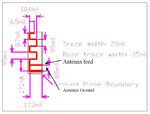
Then, I used the design of the PCB trace given by RN-171 datasheet. Their feed line was 20mil (0.50mm) width but using a 4-layer PCB, so I changed it to 1.4mm. Will my design work this way ? Do I have to change the lenght of the trace ?
One more thing I was never sure to clearly understand: should I add a ground plance on the bottom layer (antenna being on top layer) or should I leave the area around antenna (top and bottom) free from ground planes and routes ?

Untitled-1.jpg
Extract from RN-171 Datasheet - PCB Trace Design

Thank you very much
Corentin
 

Their feed line was 20mil (0.50mm) width but using a 4-layer PCB, so I changed it to 1.4mm. Will my design work this way ?

Yes. Your method is correct.

Do I have to change the lenght of the trace ?

No, the length can be unchanged.


One more thing I was never sure to clearly understand: should I add a ground plance on the bottom layer (antenna being on top layer) or should I leave the area around antenna (top and bottom) free from ground planes and routes ?

There is NO metal under the antenna area.
 

Thank you very much for your valued, clear answer Volker_muehlhaus !
Hope this will help others like me.

Corentin
 

Hi !

This is me again. So I ordered the PCB and it works well ! However, the PCB is now thin (0.8mm). After some discussions with Roving Network, they told me that the board thickness doesn't really matter. If I print my next PCB in 1.6mm thick instead of 0.8mm without changing the other dimensions of the antenna, will change my results ?

Edit:
I have very often seen sentences like: "Distance between ground and trace, trace width and dielectric material are the main factors" but my question is how can I calculate the distance between ground and trace ?

Thank you again.
Corentin
 
Last edited:

If I print my next PCB in 1.6mm thick instead of 0.8mm without changing the other dimensions of the antenna, will change my results ?

Not much, because the field of your antenna is mostly in air.
(It would be important for antennas with a ground below, e.g. patch antennas.)

I have very often seen sentences like: "Distance between ground and trace, trace width and dielectric material are the main factors" but my question is how can I calculate the distance between ground and trace ?

This does not apply to your antenna, because there is no ground below.
 

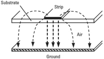
When microstrip line was proposed for the first time in 1952 everybody was making jokes when they see that this line actually radiate like an antenna due to inevitable discontinuities (compared to stripline which don't). Only in 70'ties when first microstrip antennas were proposed people starts to be happy with this radiation.
So, the radiation losses depends by dielectric constant, substrate thickness, and the circuit geometry.
Regarding the substrate thickness, thicker the substrate, higher the radiation losses. Sometimes when is looking to lower these losses a designer can suspend a thin substrate (where is printed the antenna) over a thick air space. Most of the mobile phones do this for their embedded antennas.

9223867700_1348758016.gif
 

Not much, because the field of your antenna is mostly in air.
(It would be important for antennas with a ground below, e.g. patch antennas.)


This does not apply to your antenna, because there is no ground below.


I used the board thickness to calculate the feed width. So I suppose the method I used to calculate the feed width (see previous posts) doesn't suit the application. So I need to turn back to the initial question: how can I design a Trace Antenna for a 2-layer board ? The one given by Roving Networks is only for 4-layer PCBs.

Thank you

Corentin
 

I used the board thickness to calculate the feed width.

You are right: The feed line does change, so that feed line width needs to be adjusted. On 1.5mm FR4, the required line width for 50 Ohm line impedance is 2.7mm.
 

I have a little different problem. I just need to draw a short 50 ohm feedline (not antenna) on the PCB. It is in 150MHz range. Do I need a ground plane on the other side of the board and is the trace width important at all?
I just have an RG-58 coaxial cable that connects to the PCB board, goes through a special RF relay and then exits the board.
 

If the line is short (some cm) then you don't need to care about the line impedance at 150MHz. Just avoid excessive path length in the ground, it is equally important as the "signal" path.
 
  • Like
Reactions: tarts

    tarts

    Points: 2
    Helpful Answer Positive Rating
ok thanks. How should I trace my ground connections? Jus as short track from one connector to the other as possible with no ground plane on either side?
 

How should I trace my ground connections? Jus as short track from one connector to the other as possible with no ground plane on either side?

Ground plane is fine, but not required. Short track is ok.
 

Status
Not open for further replies.

Part and Inventory Search

Welcome to EDABoard.com

Sponsor

Back
Top