bluetwin
Newbie
Good morning all,
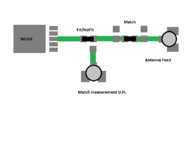
Sorry if I'm reposting a question that's been done over and over.. but I'm testing a piece of customer equipment with WLAN capability in my current contract. The WLAN chipset is on a main PCB, printed antennas on little PCBs are mounted on the plastic front panel. Antenna PCBs have a U.FL pigtail and connect to the main board U.FL socket. The engineer who designed the board has put on another U.FL socket with an arrangement of FIT/NoFIT resistors so that the S11 into the antenna can be measured... however he's calibrating the VNA tail with an SOLT, then using a SMA to U.FL to connect into the board on the "test" U.FL socket to measure the match to the antenna connected to the second socket. There are pads for matching components between the chipset and the antenna U.FL socket.
In previous lives I've always tried to copy bits of critical layout like this, plus a Short, Open and Load, onto a test coupon with a edge mounted SMA, or, if that's not been done, used either a little bit of thin semi-rigid to launch from the VNA straight onto the WLAN chip output pads, or used a Gigatest Labs station.
That way, the VNA correction can be done using the Gigatest SOL boards, or by making up semi-rigid launchers on to a bit of PCB / coupon populated with components make up SO & L. My thought is that what's going on here with this second U.FL is completely skewing the measurement by introducing additional length and discontinuity into the RF train. However I appreciate that I don't have the luxury of a Gigatest probe station here, and I don't get a perfect SOLT correction making up my own standards so errors will be introduced there.
I've attached a shonky MSPaint image of what's going on at the main PCB, sorry about the quality but it gives the general idea.
I'd love to hear your thoughts as the best way to get a meaningful baseline measurement with correction at a defined reference plane with what I have around me, so that I can get on to working out the matching network.