Continue to Site

Welcome to EDAboard.com

Welcome to our site! EDAboard.com is an international Electronics Discussion Forum focused on EDA software, circuits, schematics, books, theory, papers, asic, pld, 8051, DSP, Network, RF, Analog Design, PCB, Service Manuals... and a whole lot more! To participate you need to register. Registration is free. Click here to register now.

Overshoot and undershoot of switched type digital signal

Status
Not open for further replies.

Junus2012

Advanced Member level 5
Joined
Jan 9, 2012
Messages
1,552
Helped
47
Reputation
98
Reaction score
53
Trophy points
1,328
Location
Italy
Activity points
15,235
Hello friends,

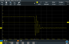
I have in my digital circuits outputs like digital signal from FPGA board or simple logic IC a practical bouncing when the output switch from one logic state to another state (from 0 to 1 or 1 to 0) as seen from the images below.
I have read from digital buffer data sheet a general note that if the output current drive capability is high, then this bouncing will be expected. I want to know from your experience how you treat it, because what I see from my eys that these over or undershoot magnitude are big enough to trigger the next logic stage.
The other question, why these peaking were not predictable by Cadence simulator.

Thank you in advance
BOUNC02.PNG


BOUNC1.PNG


Regards
 

Attachments

  • BOUNC1.PNG
    BOUNC1.PNG
    24 KB · Views: 111

Solution
I do not think you need an active probe, just make sure, if your using a DSO, your probes
are compensated both for G and response (DSOs generally have a routine to do this), and
you do the manual comp if also needed. Manuals have all this info.

No RC is needed in 99% of designs. Just attention to transmission line effects and loading
as Klaus has pointed out.

And make sure no kinks in probe cabling, and scope and probe connector to scope clean
and good contact. Lastly its ground lead length major contributor to this problem as
videos pointed out. And transmission line loading, and layout (you can "kink" a PCB
transmission line trace and create a lot of problems). Ap note son web on this topic.


Regards, Dana.
Do you have a pretty hefty ground layer? In other words your not using a trace for ground and power? If you do have healthy power planes have you put bypass Cap (Like 0.1uF) as close the ground power connections on each IC? I think your simulation program assumes this is done so the ground and power are ideal in simulation. In real world designs doing a good low noise PCB layout and doing things like having bypass caps is essential or your circuit will (As you said) trigger on noise / ringing. You could try tacking .1uF caps on the parts directly for test. Oh! How long is the ground lead on your scope? I hate admitting this but I put a long cliplead on my ground and everything looked like this.

Keep at it. Sounds like your doing pretty good with simulation which is not an easy thing. Anyway I hope this is of some help.
 
You need to properly terminate your signals. You give us no information about your layout, components or anything else useful.

Does Cadence simulator analyze PCB signal integrity?
 
Last edited:
The other question, why these peaking were not predictable by Cadence simulator.
The oscillations are well predictable with an appropriate measurement circuit model.
--- Updated ---

The oscillation frequency is unsually low, looks like large load capacitance and series inductance or long unterminated cable.
 
Last edited:
What is the time base setting in your scope shots, is it 80 ns / div ?

If so thats ~ 33 Mhz, trace osc then is ~ 1/3 of that = 42 Mhz, probe C
and L from parasitics .......

You using a 10 x probe ....?


Regards, Dana.
 
Last edited:
Look first at your VDD pin, and see if there's equal ringing
amplitude there. If so pay more attention to decoupling as
a designed thing. Too-high Q (too-low ESR and maybe too
high ESL) can make the supply rail an injection-locked
oscillator.

If supply is solid yet outputs are ringing then maybe it's
wirebond and package trace inductance, possibly making
a tank with the probe tip C. Could involve supply wire
bonds and/or the output signal bond wire. These tend
to not be "inside the chip design", often overlooked and
uninspected.

Test tis by imposing a small resistor between tip and the
point of measurement. Should be small enough to not
attenuate signal against 1Mohm or 10Mohm, maybe 1K.
If that kills the ringing without messing up edge rate
(1K, 7pF is ~ 7ns tau, probably bothers anything with
under 10ns risetime, if this is you try 100 or even 10 ohms,
observing effect on the displayed ringing.
 
Dear friends,

Thank you everyone for your kind help and response to my post, I have read all of your comments and watched the nice videos from Dana,
This will allow me to come to realize some of practical facts in my hardware

1. I am using a ground plate, but normal VDD trace. In my next design I will use four layer PCB to have VDD plane as well. Which shall reduce the noise effect and make a stronger rails

2. I am not using any type of signal termination, and to be honest, it is the first time for me to know that digital signals need also a termination technique. However, I tried today to use some of the termination technique and I could have a control over the shooting and undershooting vlotage. I used simple low pass RC filter with R=100 Ohm and C=2.2 pF. The interesting thing that this setting has to be readjusted depending on the wire length

3. I am using a passive probe, I have seen from the videos provided by Dana that active probes are more accurate to capture the real signal from my circuit. Also with the passive probe, I used direct connection possibility of the probe to make the ground cliplead shorter, and the peaking effect was improved

Thank you once again and looking forward to your comments on my pointsd
Best Regards
 

Hi,

1) did someone mention you need a VDD plane? Usually a GND plane combined with proper decoupling capacitors is sufficient.

2) it´s an signal echo. The return time depends on the length. Quite expectable.
If you are doing a proper signal transmission line (with proper characteristic impedance) combined with a proper terminiation then there is no echo. No echo --> no need for an adjustment.

3) Did someone speak of active probes? A (recommended) 10:1 divider probe is not "active". It´s just two resistors and a trimming capacitor.

For more detailed answers to your problem it would be very helpful to see some photos of your wiring and setup.

Klaus
 
I do not think you need an active probe, just make sure, if your using a DSO, your probes
are compensated both for G and response (DSOs generally have a routine to do this), and
you do the manual comp if also needed. Manuals have all this info.

No RC is needed in 99% of designs. Just attention to transmission line effects and loading
as Klaus has pointed out.

And make sure no kinks in probe cabling, and scope and probe connector to scope clean
and good contact. Lastly its ground lead length major contributor to this problem as
videos pointed out. And transmission line loading, and layout (you can "kink" a PCB
transmission line trace and create a lot of problems). Ap note son web on this topic.


Regards, Dana.
 
Last edited:
Solution
A FET probe imposes much less tip capacitance on
the circuit. If ringing frequency responds to that then
you can conclude it's happening at the pin and
involving close-in parasitics as the "tank".

But many FET probes are very limited in signal range,
being meant for sensitive / small signal RF stuff. So
might read that instruction manual's operating table
before you blow up something expensive (or just get
results that are badly clipped).
 
I still wonder which passive probe configuration achieves this low oscillation frequency. Is it a 1:1 probe with respective large input capacitance?

Although it's generally difficult to reproduce ns risetime signals exactly with passive probes, you can achieve much better results with almost no overshoot. Ultimately solder special coaxial jacks to the circuit that directly connect to the probe tip. Active and low impedance resistive probes (e.g. 1k 20:1) achieve nevertheless better signal quality, even with moderate length (< 5 cm) ground clips.
 
Dear Friends,

Thank you very much for your explanation.

I see you all agree to use 10X probe, and actually I was using 1X probe with long ground clip lead

two things improved my measurements based on your help:

1. I used 10X probe, I am little shy to tell that I was not aware how 10X probe properties are far better than 1 X probe properties in terms of bandwidth and loading effect on the DUT (less capacitance and higher resistor). For the probe I am using it is 10X: 10M Ohm || 10 PF

2. I used the short spring metal instead of the ground lead

3. I have implemented the manual probe compensation

After this I have also noticed, but expectably that if I am transferring signal over wire, the peaking effect at the end is a function of the wire length, which also come to the point you mentioned, which the wire/trace conductance effect

Thank you for your help
Best Regards
 

Ultimately solder special coaxial jacks to the circuit that directly connect to the probe tip.

I have been holding onto a couple of scope probe jacks
from old Tek probes, but I haven't found anything suited
to the more modern ones that came with my TDS3054.
I gather that those probes may be partially disassembled
to get at the ground shield that's usually not exposed.

But still, I have not seen a source for a solderable jack
that's meant to fit.

Anybody got a lead?
 

Most recent passive probes have 5.0 or 2.5 mm tip with coaxial ground contact. They are often shipped with BNC adapter. Solderable coaxial 5.0 and 2.5 mm sockets are available on the market, e.g. from PMK. We are buying them from datatec.
 

Hi,

as you already mentioned, the spring is a good way to reduce the swinging, see here [1].

I also used the connector shown below, availabe for Lecroy probes (probe: PP023; connector: PK5-2.5MM-113). Sorry, I couldn't find a better picture. With that one, it is possible to solder short or if required longer wires to the center pin and GND. Than you can even twist the wires. If protected with a shrinking tube, this connectors are quite handy to make measuremnts.

lecroy PK5-2.5MM-113.png


[1] https://assets.nexperia.com/documents/application-note/AN90004.pdf

BR
 
Mouser #: 372-N4838A
Mfr. #: N4838A
Mfr.: Keysight
Test Probes Ground Spring 2.5mm, kit of 2
$15.39

Mouser #: 372-N4827A
Mfr. #: N4827A
Mfr.: Keysight
Test Probes PCB Socket Adapter, kit of 2
$15.39
 

Dear friends,

Thank you once again for your nice information, my measurement has improved.

I see you friends suggested the Probes PCB Socket Adapter, like the one shared by freebird (Mouser #: 372-N4827A), which certainly creates an excellent measurement point to the oscilloscope.

But I have a question about it, why not instead of soldering the Probes PCB Socket Adapter, I will solder a BNC or SMA connector on my new PCB board, then I can use a coaxial/SMA cable directly without a probe ?

May be the only thing I can loose is the 10M Ohm of the 10:1 probe, but it is ok for me to have the oscilloscope input impedance of 1 M Ohm since I am testing the input and output signals, nothing in between the circuit.


At the same time, I am not sure if using the BNC/SMA connectors should be done without additional circuitry (for example termination) or not.


These are the connectors I mean

Thank you in advance

Best Regards

https://de.aliexpress.com/item/1005...ePPC__xxxxxx__1674393171&gatewayAdapt=glo2deu

https://de.aliexpress.com/item/1005...vid=202301220514273417821467016100014179972_4
 

Hi,

your coaxial cabel will actually act as a capacitive load with usually ~100 pF/m e.g. [1]. Further, the characteristic wave impedance of your coaxial line is 50 Ohm. To avoid reflections you would have to terminate the line with a 50 Ohm resistor at your scope side (or you have a scope where you can switch to a 50 Ohm input). This depends on the used coaxial line length as well as measured frequencies. Based on this considerations, the circuitry under test will be most likely heavily influenced, as your probe does not represent a high impedance, and your measurement result does not display the actual situation.

[1] https://www.farnell.com/datasheets/...43.182990577.1560099811-1902511469.1560099811

BR
 

Status
Not open for further replies.

Part and Inventory Search

Welcome to EDABoard.com

Sponsor

Back
Top