Sam315
Newbie
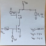
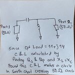
Hello, Can anyone help me with the concept of how to do the output matching network of a class A PA. My S21 is 12dB and my S11 is matched at 60GHz. I have performed the load-pull simulation and found that the optimum load is like 11+j14. Now, what should be the next step to determine the output matching considering the optimum load? I have read in many papers that there should be conjugate matching in order to get the maximum efficiency but I am confused about how to do that conjugate matching in my design. If possible please help me.
--- Updated ---
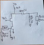
A further approach that I have done is I used that optimum load and calculated capacitance and inductance according to that. But in the end, if I place it in the circuit connecting Vdd and the following inductor my gain reduces. I am so confused about where I am doing wrong!Hello, Can anyone help me with the concept of how to do the output matching network of a class A PA. My S21 is 12dB and my S11 is matched at 60GHz. I have performed the load-pull simulation and found that the optimum load is like 11+j14. Now, what should be the next step to determine the output matching considering the optimum load? I have read in many papers that there should be conjugate matching in order to get the maximum efficiency but I am confused about how to do that conjugate matching in my design. If possible please help me.
Attachments
Last edited: