Continue to Site

Welcome to EDAboard.com

Welcome to our site! EDAboard.com is an international Electronics Discussion Forum focused on EDA software, circuits, schematics, books, theory, papers, asic, pld, 8051, DSP, Network, RF, Analog Design, PCB, Service Manuals... and a whole lot more! To participate you need to register. Registration is free. Click here to register now.

OTA sizing by gmoverid approach

Status
Not open for further replies.
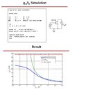
The 1st graph, try sweeping the current to a larger value say 500uA or 1mA to see the full curve. I don't know what the size of the MOS is maybe you are not getting out of subthreshold with 1uA of current.
When they say gm/Id is region independent I think they only mean its independent of subthreshold-weak inversion-saturation. When the MOS goes into triode the the gm/Id curves I saw were not very consistent and varied all over the place as soon as I started nearing subthreshold.

What is Iref in the 1st graph? Is it the sweeping DC current source? If that is the case then when you plot gmoverid vs Id/(W/L) that should only change the scale of the x-axis and not the shape of the graph since W/L is constant throughout the sweep, right?
So it could be that something is going wrong in the Cadence plotting AWD. I myself could never get the plots to work in Cadence alone since it kept messing up when I changed the x-axis, I then simply ended up exporting the data to MATLAB/excel and did the plots much more easily.
 

yes, Iref (Id )is being swept in the 1st graph, which is the value of current source,

only change the scale of the x-axis and not the shape of the graph since W/L is constant throughout the sweep, right?
True, it only scale change, curve remains the same !

omething is going wrong in the Cadence plotting AWD. I myself could never get the plots to work in Cadence alone since it kept messing up when I changed the x-axis, I then simply ended up exporting the data to MATLAB/excel and did the plots much more easily.
Data can be easily be exported using oceanscript. I will check if theres is a change with matlab !

Could it be, that cadence is unable to do multiple sweeps here, and it cannot handle ID/(W/L), because there are essentially three variables to sweep.
All One variable graphs on x-axis ARE PERFECT as opposed to multipled variables design variables like ID/(W/L) !!
 

Hi, EmbdASIC,

In EE214, gm/id simulation test bench is in the attachment.
Also, in EECS240, gm/id simulation test up is using a diode connected NMOS and sweeping the Vds.

You can try both.

Best Regards
 

Hello

Sorry to interrupt you guys but one question is really troubling me, In Murman notes, he has designed a 2 -stage OTA by using gm/id methodology.

Now two things are bothering me since I haven't been able to understand how exactly are they working.

1) How did he get the Length(L) of the transistor by using intrinsic gain charts? Lets say that I write an ocean script and save all the required parameters like gm , ro etc . How can I come up with the required length of the transistor?


2) The second thing is about the "reference gmoverid parameter" which Jasper has mentioned as (gm*/id*) in his book ? How can we calculate this reference gmoverid parameter. Does it mean that we can simply fix the length and the width of our transistor under consideration to some arbitrary value?


I would be really grateful if someone could answer my question.
 

hello,

@holddreams:
the problem was not the simulation testbench, neither few of those easier curves such as gmoverid VS id OR gmoverid VS Veff etc... BUT to obtain the famous gmoverid VS ID/(W/L) as shown in fig.1 of the attached paper !!
So if somebody has done it preferrably without leaving the cadence domain, PLEASE come forward with suggestions !!

@kakajeej
According to Jespers et.al you need two graphs to get your transistor dimensions:
1. gmoverid VS Id/(W/L) graph to get W/L
2. gmoverid VS Vearly graphy to get L.
Now the other parameters are dependent upon your design requirements and would automatically be obtained if the above two graphs are somehow obtained for your process.

The Attached tutorial will help you find your gmoverid easily! it has helpful tips !
but could you post a link to murmann notes you are reffering to !
 

I use Cadence composer to draw schematic, Virtuoso to draw layout, spectre and spectremdl to run simulation.

Change the testbench in EE214 to spectre format, record the gmoverid, ids, etc ,and can easily get the waveform just like in the paper.

1)Edit "gmid_nmos_ee214.scs"

//NMOS gm/id simulation
simulator lang=spectre insensitiv=yes

//global parameters
global 0

//include model files
include "./tsmc011.scs" section=tt_33
include "./macro.scs"

//include netlist
xmn (d g 0 0) n2 w=10 l=0.5 m=1

//parameters
parameters pwrvgs=1.8

//stimulus
vd (d 0) vsource type=dc dc=1.65
vg (g 0) vsource type=dc dc=pwrvgs

//options
Setoption options scale=1u
SetTempoption options temp=25

//output option
sppSaveoptions options save=allpub

//Alter groups
Alter_tt altergroup {
include "./tsmc011.scs" section=tt_33
}

2)Edit "gmid_nmos_ee214.mdl"

alias measurement finddc {
run dc
export real ids, gm, gmoverid, vstar, vstar1, idsoverwl
ids=xmn.n:ids
idsoverwl=ids*0.5/10
gm=xmn.mn:gm
gmoverid=xmn.mn:gmoverid
vstar=2/gmoverid
vstar1=2*ids/gm
}

foreach pwrvgs from swp {start=0.01, stop=3.3, step=0.1){
run finddc
}

3)run "spectremdl -batch gmid_nmos_ee214.mdl -design gmid_nmos_ee214.scs"
4)open "wavescan&"
5)In the wavescan window,open "gmid_nmos_ee214.raw",
6)click "finddc_meas-meas_foreach",click "gmoverid", then click top-left "Y Vs Y for two signals", and then click "idsoverwl"
7)In the waveform showup, click x-axis, chosse "scaling--log", click "ok", and can easily get the waveform just like in the paper.

Attached is the testbench and waveform in ee214.
 

Attachments

  • gmid_nmos_ee214_simulation_1395.jpg
    gmid_nmos_ee214_simulation_1395.jpg
    111.3 KB · Views: 115

If you sweep Vgs from 0.01V to 3.3V with a Vds set to 1.65V, then at some point the transistor will leave saturation. (e.g. Vgs > Vds + Vt) I assume in this case the gm values become questionable.
In normal design scenario's, does this pose a problem?

So do you reccomend sweeping the Vgs to a more limited range so as not to leave saturation, or are you better off setting Vds to a higher value, e.g. Vds > Vdd - Vt ?
Equally are these reasons why you also see people using the diode connected mos configuration?
 

Hi thiery,
Yes this is why the diode connected configuration is best. In this if you add a voltage source from the gate to drain and sweep its value from say -0.3 to +0.3 you can also get variation in the drain voltage and see how that affects it. Till the time you have the transistor in saturation the gm/Id vs Id/(W/L) curves are very consistent.
 

Status
Not open for further replies.

Part and Inventory Search

Welcome to EDABoard.com

Sponsor

Back
Top