Continue to Site

Welcome to EDAboard.com

Welcome to our site! EDAboard.com is an international Electronics Discussion Forum focused on EDA software, circuits, schematics, books, theory, papers, asic, pld, 8051, DSP, Network, RF, Analog Design, PCB, Service Manuals... and a whole lot more! To participate you need to register. Registration is free. Click here to register now.

Op-amp based current source ckt has a problem

Status
Not open for further replies.

arup

Member level 2
Joined
Sep 6, 2004
Messages
46
Helped
0
Reputation
0
Reaction score
0
Trophy points
1,286
Activity points
441
Hello,

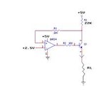
Below is the current source ckt for thermistor( RL).
untitled.JPG

I am using the current source(approx 0.1mA) to excite the thermistor(RL). RL = 100 Ohm .When I check (+) terminal of opamp with oscilloscope ,the waveform found oscillating (Saw tooth like waveform, mean value 2.5V DC but pk value 4.0V ).
What causes the oscillation.How to resolve the issue.
 

Using positive feedback usually results in an oscillator.
It's still negative feedback (inverting operation of Q1), but unstable due to the additional loop gain provided by Q1. The circuit needs addition compensation, e.g. a capacitor from OP output to negative input, in combination with a resistor to 2.5 V reference. Or redesign it with a PNP transistor and flipped OP inputs.
 

My mistake - I was thinking of the more conventional emitter follower based output stage. As you say, a PNP and reversing the opamp inputs would be a good option.

Keith
 

One thought - depending on the current accuracy you require you might be better to use a MOSFET. Emitter and collector currents are not identical.

Keith
 

It's still negative feedback (inverting operation of Q1), but unstable due to the additional loop gain provided by Q1. The circuit needs addition compensation, e.g. a capacitor from OP output to negative input, in combination with a resistor to 2.5 V reference. Or redesign it with a PNP transistor and flipped OP inputs.

Can you plz explain how the ckt works? And why it's oscillating?
i understands that at the power up ,transistor ( here 2N2222A) will not be on .with a Dc i/p of 2.5V at -ve terminal of op-amp , op-amp o/p will force the transistor to switch on such a way that thru' R1(+ve feedback ??) voltage at +ve terminal become 2.5V.But why i don't see pure DC neither at pin no 3 nor at pin 1. there are saw tooth like waveform.It's like transistor is getting ON & OFF .correct me!!
Could u plz comment in more detail?

thnks,
 

I assume that you know how the circuit works, except for the stability issue.

Q1 is working as an amplifier in common emitter configuration with a voltage gain of about 70. It's acting as feedback factor for the OP. Standard OPs are not compensated for feedback factors > 1.
 
  • Like
Reactions: LvW

    LvW

    Points: 2
    Helpful Answer Positive Rating
Thanks all for ur valuable comments.yes, I have re-designed it using PNP transistor.

rgds,
 

Status
Not open for further replies.

Similar threads

Part and Inventory Search

Welcome to EDABoard.com

Sponsor

Back
Top