vijayaganesh
Newbie level 5
- Joined
- Oct 2, 2013
- Messages
- 9
- Helped
- 0
- Reputation
- 0
- Reaction score
- 0
- Trophy points
- 1
- Location
- Tuticorin(Thoothukudi), India, India
- Activity points
- 49
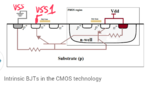
Can anyone explain clearly how NTAPS and PTAPS can solve the latchup effect by fabrication point of view? And one more thing its the only job for PTAPS and NTAPS