Continue to Site

Welcome to EDAboard.com

Welcome to our site! EDAboard.com is an international Electronics Discussion Forum focused on EDA software, circuits, schematics, books, theory, papers, asic, pld, 8051, DSP, Network, RF, Analog Design, PCB, Service Manuals... and a whole lot more! To participate you need to register. Registration is free. Click here to register now.

Negative signal conditioning for sampling with battery powered A/D

Status
Not open for further replies.

jlewis184

Newbie level 3
Joined
Feb 21, 2009
Messages
3
Helped
0
Reputation
0
Reaction score
0
Trophy points
1,281
Activity points
1,306
I'm designing a microcontroller application for controlling LEDs. The application is battery powered and the micro is running at +5V.

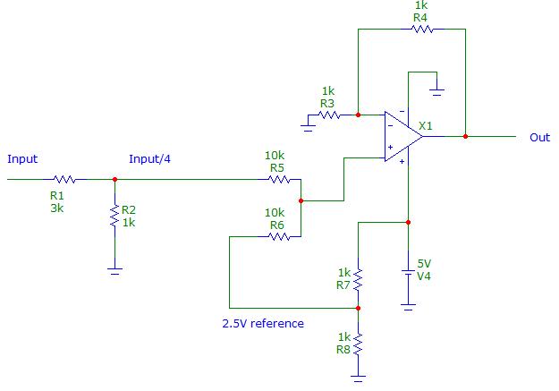
I need help on conditioning an input signal to the A/D of the micro. The input is a control voltage (CV) from Eurorack synthesizer module, and swings +/- 10V. I want to offset and scale this 20Vpp signal to 0 to 5V, for sampling with the micro.

Can someone explain how to do this with a single, 5V positive supply? I think I need a rail-to-rail opamp, with virtual GND at 2.5V, and use a voltage divider to scale the input....but I'm not too clear on the details.

Thanks,
Josh
 

You have to divide the input by 4, in order to have a signal that swings between +/-2.5V, then add to this 2.5V in order to have a signal in the range 0, 5V.

In the input impedance of your ADC is quite high you can use only a resistive network, otherwise a buffer based on rail-to-rail opamp have to be used. For instance:


Be carful to the tolerance of resistance if accuracy is required. If you don't need low impedance you can remove the opamp, R3 and R4, so your output will be the node now going to the non inverting input of the opamp.
The value of resistors are just an example. if you need less current to be absorbed from the input (now is quite high) you can increase R1 and R2. However in this case you'll have to increase also R5 and R6 that have to be equal one each other and much greater than the greter between R1//R2 (// stand for parallel) and R7//R8.
 

    V

    Points: 2
    Helpful Answer Positive Rating
Sorry, I think there are problems in using only the resistive network as is. I'll correct it asap.

OK, the problem is that the op-amp has a gain of 2, then using the resistors network alone you will have half of the voltage you need. To resore the correct range you have to lower the input divider ratio from 4 to 2 (f.i. decreasing R1 from 3k down to 1k) then you have to do the same at reference side where the divider ratio has to be, now, 1 (f.i. short circuiting R7).
 
Last edited:

Can this circuit work like you suggested earlier, without the op-amp and taking the output at node R5 & R6.

Or can the op-amp be configured with unity gain, and the scaling left as is? ....R4 = 0 ohms.
 

You can use either the circuit in the picture, with opamp (gain=2), or the circuit with only resistors, but with the ratio modified as per post #3. I apologize for the confusion I did.
 

Can this circuit work like you suggested earlier, without the op-amp and taking the output at node R5 & R6.

Yes, this works if your micro A/D has a rather high load resistance ( » R5||R6 ).


Or can the op-amp be configured with unity gain, and the scaling left as is? ....R4 = 0 ohms.

Yes, with this configuration you can achieve a much lower output impedance. I'd recommend more higher resistive resistors, though, see this figure:
level-shifter.gif

In this case you'd need a real output rail-to-rail opAmp, of course.
 
Thanks for your reply erikl. What program are you using to simulate this design?

I would also like to the ability to switch off/on the offset voltage applied. If I simply switch R6 out of the circuit, I think the impedance is mismatched at the input of the op-amp :?:. Can you recommend a simple solution?
 

Hi Jerry ;-)

What program are you using to simulate this design?
Qucs - quite universal circuit simulator. SPICE based free software.

I would also like to the ability to switch off/on the offset voltage applied. If I simply switch R6 out of the circuit, I think the impedance is mismatched at the input of the op-amp :?:.
You mean: remove R6 ? In this case there's no offset and total gain=½ , i.e. you transfer 0≦Vin≦10V --> 0≦Vout≦5V ; at the intersection of R1 & R2 of course you get -10V≦Vin≦10V --> -5V≦Vout≦5V.

As to opAmp input impedance mismatch: yes, R3=(R5||R6), i.e. R3=R5 in this case. But it's not so important if R3=½*R5 , as an input voltage offset caused by this mismatch is amplified only by a gain=1 , makes less than 1mV with low input current opAmps.

If you'd connect R6 to GND, again no offset, but total gain=0.247≈¼ , you transfer 0≦Vin≦10V --> 0≦Vout≦2.47V .
 
Status
Not open for further replies.

Similar threads

Part and Inventory Search

Welcome to EDABoard.com

Sponsor

Back
Top