sjamil02
Member level 4
- Joined
- Nov 8, 2009
- Messages
- 72
- Helped
- 9
- Reputation
- 18
- Reaction score
- 5
- Trophy points
- 1,288
- Location
- United Kingdom
- Activity points
- 1,961
Dear All,
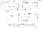
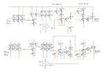
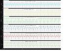
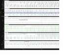
I am designing a push-pull regulator for digital circuits. The schematic is as attached. It consists of pre-amplifier followed by comparators (push and pull side) and finally switched source-follower output stage (push and pull side). I have verified that all the feedback loop (pre-amp for cmfb and replica bias loop for push and pull side) are stable with reasonable gain (around 30dB). Also the comparator include internal hysteresis that set the deadband around 60mV. For transient simulation setup, I put in a dropper resistor and load current from 0mA-->5mA @5MHz. This is to emulate VDD variation when there is a load current variation. The simulation results came out to be incorrect. As you can see from the attachment, only push-side of the transistor is drawing current and the pull side is off (only draw very small current). And also the VREF value is much lower than VDD. I am expecting VREF to be at average value of VDD but seems that from the simulation, this is not the case. I have spent a lot of time trying to trace the problem but still couldn't get any clues.
I hope someone can enlighten me and give some valuable advice. Please help me.
P.S./ Hope the schematic and simulation results are visible enough. Please let me know if you want to know more information about this design.
Thanks