Continue to Site

Welcome to EDAboard.com

Welcome to our site! EDAboard.com is an international Electronics Discussion Forum focused on EDA software, circuits, schematics, books, theory, papers, asic, pld, 8051, DSP, Network, RF, Analog Design, PCB, Service Manuals... and a whole lot more! To participate you need to register. Registration is free. Click here to register now.

Need help in simulation

engr_joni_ee

Advanced Member level 3
Joined
Nov 3, 2018
Messages
750
Helped
2
Reputation
4
Reaction score
4
Trophy points
18
Activity points
6,231
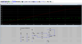
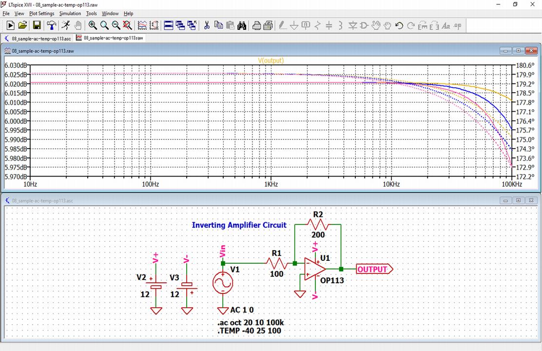
Hi, I am trying to run the simulation in LT Spice but I am not sure what is missing.
Can someone please have a look and suggest what can be done to run the simulation.

Untitled 648.png
 
I am not sure if I get the step width.
The simulation should be done at 1000, 1200, 1400, 1600. There should be only four points in vout calculation.
 
I got this :
OP used: (referenced to schematic of post#20)
* R1 = 1k
* R3 = 10k
* AD8397
* chart R_Pt vs output

Thus the results are hard to compare / validate.

Btw: can any one find the Common Mode Input Voltage range in the AD8397 datasheet?

Klaus
 
The simulation should be done at 1000, 1200, 1400, 1600. There should be only four points in vout calculation.
Your decision, but why are you complaining that "the red curve Vout is piece wise linear"? Piece-wise linear ist just the backside of plotting only 3 segments. If you plot more segments, you'll immediately see in which way the transfer curve is nonlinear. You'll realize that the amplifier can't linearly process the input voltage range.

You can even see it by analyzing the three segment plot. If you extrapolate the line connecting point 2 - 4, you notice that point 1 corresponds to an output voltage < 0.
 
Hi,

but ...
* schematic of post#17 is´t even from OP

and the resistor values make no sense for a difference amplifier circuit. (not your fault):
For a difference amplifier R3 shoud be equal to R4 and R1 should be equal to R2.

To get perfect CMRR R2 needs to becoorected by source resistance.
And then the ratio of the inverting side and the ratio for the non inverting side needs to be equal.

Klaus
 
@KLAUS, was I ever out to lunch. But post # 17 looks like a single ended design
to me, trying to be a NINV amp with a complicated attenuator at input. As is
post #1. But then R values making one think its differential (Post #1), until one realizes
its got a 1.02 V bias not presented as CM, both posts.

Sort of a Mad hatter tea party design.......

Or maybe I should take a nap.....and let the experts figure this one out.

One thinks of using a bridge, but deviation of PT so large it needs linearization :


Regards, Dana.
 
Last edited:
Hi,
to me, trying to be a NINV amp with a complicated attenuator at input. As is
post #1. But then R values making one think its differential (Post #1), until one realizes
its got a 1.02 V bias not presented as CM, both posts.
Different views. Without saying the one view is more correct than the other.

I personally often recommend the "difference amplifier circuit" like in post#1, especially for newbies.
I see nothing wrong in applying a fixed 1.02V bias on one input of the difference amplifier.

It´s rather universal, and easy to use.
* you can use it true differentially
* or single ended
* you may use it as true amplifier or as attenuator
* you may invert an input signal or not
* you may add or subtract offset
One problem with this circuit is, that it expects low impedance input sources.
And this - I think - is what worries the OP. The OP calculates the PT voltage .. but ignores that "this source" is rather high impedance, so the circuit´s input current (input resistance) modifies the PT voltage.

And here (post#9) I asked the OP to do some simple investigations on his own ... to find out that it´s not only the output voltage that is unexpected, but it´s even the PT voltage that is unexpected. One does not need a simulation tool for this. But if there is, one can use it to measure nodes. (Paper and pencil is sufficient, or excel..)
The OP did not communicate to post#9, so I assume he more wants to discuss with other forum members. There´s nothing worong with it.

You already know I have my own forum style, where I expect the members to be eager to learn and to do simple debugging/investigating steps on their own.
There are many people who like this style a lot, and they learn for life, don´t need to ask a similar question again, because they´ve learned to find the solution on their own.
But there are also a lot people that don´t like my style, maybe because they expect a ready made solution .. which I usualy don´t provide. And that´s OK for me, too.
I´m not the one who does basic Ohm´s law calculations for them over years.

Klaus
 
Hi, I got something working using the same differential amplifier configuration i.e, subtracting a voltage 0.9 V (this can be taken from voltage reference) and a gain of 7.8 times. The output voltage is plotted using smaller step between PT = 1000 Ohm and PT = 1600 Ohm. I guess this represents 0 degC (1000 Ohm) and 158 degC (1600 Ohm). he output voltage looks linear.

Is that circuit practically possible to make on a PCB with real components ?

How much the device characteristics of AD8397 changes itself with temperature ?
 

Attachments

  • Untitled 663.png
    Untitled 663.png
    49.8 KB · Views: 15
Last edited:
As you can see the output looks saturated at PT = 1000 ohms. OpAmp
is meant for driving heavy loads, and data sheet clearly indicates there
are limitations at -Swing. You can fix that with a LV - supply or better
yet different choice for OpAmp.

Note also, as previously pointed out by Klaus, there is no input CM Range spec.
In fact input R is quite low for an OpAmp at 87K typical.

1713955737997.png


I ran it with more output load, no significant difference.


Regards, Dana.
--- Updated ---

Effects of T from 20C to 50C, mainly affects low end of PT range :

1713957684993.png


Regards, Dana.
 
Last edited:
Hello Dana,

Thank you very much for your comment. Kindly explain bit more as you said you can fix that with a LV - supply or better. Would you please suggest changes to be done in the circuit provided we keep the same device.

I understand the output is saturated at PT 1000 Ohm. How about the output at PT = 1100 Ohm ? Our range of temperature start from room temperature so I guess if we get an output starting at PT = 1100 Ohm then it's also fine.

You also mentioned common mode range. I guess it is not provided in the data sheet of AD8397.
 
Yes PT 1100 ohms past the sat point. The sat worst case load affected spec
seems to indicate you should be OK.

1713959907442.png


And you would not need a - supply.


Regards, Dana.
 
Thanks for your comment.

How do we run thermal simulation in LT Spice. I mean to calculate the device output as a function of device temperature.
 
Last edited:
I manage to run .TEMP commands.

1- How do we set cursor on different curves ?
2- How do we know which curve is representing which temperature ?
3- Is that possible to export the data of four curves in text file ?
 
Last edited:

LaTeX Commands Quick-Menu:

Similar threads

Part and Inventory Search

Welcome to EDABoard.com

Sponsor

Back
Top