Continue to Site

Welcome to EDAboard.com

Welcome to our site! EDAboard.com is an international Electronics Discussion Forum focused on EDA software, circuits, schematics, books, theory, papers, asic, pld, 8051, DSP, Network, RF, Analog Design, PCB, Service Manuals... and a whole lot more! To participate you need to register. Registration is free. Click here to register now.

[SOLVED] [MOVED] ADS1118 interfacing to pic30f by using SPI

Status
Not open for further replies.
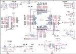
Schematic for my code

11.png
 

Its looks ok, either we have to go through the data sheet, or try changing some other ADS118 if available.
 

Hi,

connect as short as possible a 10nF capacitor between GND (of ADC) and AIN1.

Because the ADC has a switched capacitor input stage you need a low impedane source for high freqencies. --> 10nF should be OK.

the 100n ceramic is already connected as short as possible at VDD and VSS of ADC ( hopefully). An additonal 1u ceramic may additionally stabilize supply.

Klaus
 

There is a mistake in your MUX configuration you are measuring between Ain0 and Ain1(instead of gnd)
change the code for MUX[2:0] as 100 or gnd Ain1 pin thats all.

after that remove calibration

Code C - [expand]
1
//     result += 3087


The diode I said is inside your ADC
1.JPG


2.JPG
 

Hi,

In my post #23 it should be " AIN0" instead of the written AIN1.
(I try to correct this)

Klaus
 

hi KlausST and Venkatesh_M thanks for your support

My code is absolutely working fine now with tens of Micro Volts (below 0.5 Milli Volt) variation ...


Some changes done in my hardware:

1) ADS1118 A1N1 is connected ground so the disturbance coming from the GND plane would be removed.

2) Added 2 series resistance(1k each) in the digital signal lines instead of using the pull-ups


Some changes done in my Software:

1) Removed previously added calibrated value (3084),No need calibrate
 

1) ADS1118 A1N1 is connected ground so the disturbance coming from the GND plane would be removed.

That is not worked due to disturbance, read #24. Thats a wrong MUX configuration.
 

Hi

Look out, he also said the same as i did in #24 :wink:

Capture.JPG


what diff you got in these?

Here is nothing to do but proper configuration register setting, the first thing I seen in the datasheet is that error. thats all.
 

:thumbsup: ya i agree with you Venkadesh_M now i got clear view ... thanks again.....
 

MPLAB8.88V
dsPIC30F3013
C-30, V3.31

Hi,

I am trying to do the same thing as Thota suresh did. I mean reading the voltage from a 10k pot with the help of ADS1118 which is interfaced to my controller.

I have configured the single ended channel[AN3-ANP ,AN2-GND].

I'm obtaining a constant voltage ( 0.7076 mV) as output, while i'm varying the pot.

here is my SPI communication as suggested by Venkadesh_M
unsigned short int result1 = 0;
double digi_result1 = 0;
CS = LOW;
WriteSPI2(0xF003); // FOO3 when AIN3 is AINp and AIN2 is GND
while(!SPI2STATbits.SPIRBF);
result1 = ReadSPI2();

WriteSPI2(0xF00B);
while(!SPI2STATbits.SPIRBF);
ReadSPI2(); // dummy read of config register read back format and output result
while(PORTGbits.RG7); // Wait for DOUT/#DRDY to go low
CS = HIGH;
// printf("B1 = %u\n",result1);

if( result1 & 0x8000 )
digi_result1 = 0;
else
digi_result1 = digi_result1 + (((float)result1 * 6.144) / 32767U);
printf(" V1 = %.4f mV\n",(double)digi_result1);
digi_result1 =0;
result1 = 0;
PGA[0:2] = 000; // fs is 6.144 as my reference voltage is 5v
MUX[2:0] = 111;

can any one suggest me what may be the reason?
 

Hi,

please show ADC and your pot connection diagram.

Klaus
 

Hi KlausST,
Thanks for your reply,

sorry for the mistake

dspic30f5011 instead of dspic30f3013. The schematic is same as below instead of A1N0, I have connected A1N3 to pot

schemaic.png

- - - Updated - - -

my schematic

IMG_20150817_165458.jpg


And im obtaining the same result in all other channels also.
 

The schematic has SCLK and SS flipped, I guess not the real circuit.
 

Hi,

Yes, FvM found the mistake, i think.

Another hint: For those low_frequency_signal measurements it is always good to place a capacitor between analog input and ground.

Klaus
 

Hi FvM,

here is my schematic,refer the circuit with respct to U7.
ads1118.jpg

My Hardware is as per the circuit I uploaded. Clock is directly connected to Clock w.r.t master and slave, Data lines are swapped i.e DIN - DOUT, SS is pulled low and the other communication lines are pulled up with 4.7 K resistor.


How to confirm weather communication between slave and master is success or not.

Thanking You,
Khaleel Arya
 

Reveals that the post #21 schematic is incorrect, as already guessed. No problems can be recognized in the actual circuit at first sight.

In the post #31 code, you are waiting for DRDY assertion after reading the ADC data (sending 16 clocks), which won't ever happen according to the datasheet. Instead the DRDY event can be detected if sending either 0 or 32 clocks after taking CS low.
 

Hi,

Thanks for your support

Firstafall Im getting buffer value as constant(3493) while i'm varying the pot.
 

Which channel you are trying to read, can you show the part of code you have been using ?
 

Hi venkadesh,

my configuration is for AN2

Code:
CS = LOW;
	WriteSPI2(0xE003);			// E003 when AIN2 is AINp, FOO3 when AIN3 is AINp
	while(!SPI2STATbits.SPIRBF);
	result1 = ReadSPI2();

	WriteSPI2(0xE003);
	while(!SPI2STATbits.SPIRBF);
	ReadSPI2(); // dummy read of config register read back format and output result
        while(PORTGbits.RG7);
	CS = HIGH;
 

Status
Not open for further replies.

Similar threads

Part and Inventory Search

Welcome to EDABoard.com

Sponsor

Back
Top