Welcome to our site! EDAboard.com is an international Electronics Discussion Forum focused on EDA software, circuits, schematics, books, theory, papers, asic, pld, 8051, DSP, Network, RF, Analog Design, PCB, Service Manuals... and a whole lot more! To participate you need to register. Registration is free. Click here to register now.
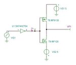
I used the structure in attached image to generate voltage swing from +5V to -5V.
But why the simulation results can not reach +5V and -5V.
Which parameters determinate the voltage swing, is it Darin to Source voltage?
The mosfet is controlled from the Vgs voltage, in Nmosfet the gate has to be higher than the source and in Pmosfet the gate has to be lower than the source.
What are you trying to do with your circuit?
IRF9130 has a gate threshold voltage of 2v min and 4v max, since you have already applied a positive voltage (5v) to the source the gate voltage needs to be the source voltage +2 to +4v (7v to 9v or higher).
The same thing applies to IRF120, it has a gate threshold voltage of 2v min and 4v max, you have applied a negative voltage (-5v) to the source so the gate should have -3v to -1v or higher.
If you are trying to do a sold state switch it should be like this
Never look at the threshold voltage when the Mosfet conducts only 0.25ma. Instead look at the R-on resistance when the gate to source voltage is 10v which dosn't happen in the original circuit.
Making the Mosfets as source-followers makes it worse because then the gate voltage swing must far exceed the output voltage swing and be 20V p-p more.
You need a level-shifting transistor to provide enough gate voltage swing.
Voltage at node VF2 should equal +5 or -5 volts for one of the transistors to be completely of.
So check if you get the said voltages at VF2....this is for the case assuming that you have no load at the VF1 node
This site uses cookies to help personalise content, tailor your experience and to keep you logged in if you register.
By continuing to use this site, you are consenting to our use of cookies.