Continue to Site

Welcome to EDAboard.com

Welcome to our site! EDAboard.com is an international Electronics Discussion Forum focused on EDA software, circuits, schematics, books, theory, papers, asic, pld, 8051, DSP, Network, RF, Analog Design, PCB, Service Manuals... and a whole lot more! To participate you need to register. Registration is free. Click here to register now.

Mosfet Inverting full bridge problem

Status
Not open for further replies.

Nasib.Fahim

Newbie level 4
Joined
May 31, 2022
Messages
7
Helped
0
Reputation
0
Reaction score
0
Trophy points
1
Activity points
48
Hi all. I have a problem.

I am using this circuit to invert the current sense just with one command line (I1).

If i use this circuit as it is, somehow i am seeing a short circuit somewhere. If i reduce the 15V to 5V the circuit works correctly.

Could anyone help me please ?

Thanks a lot!!
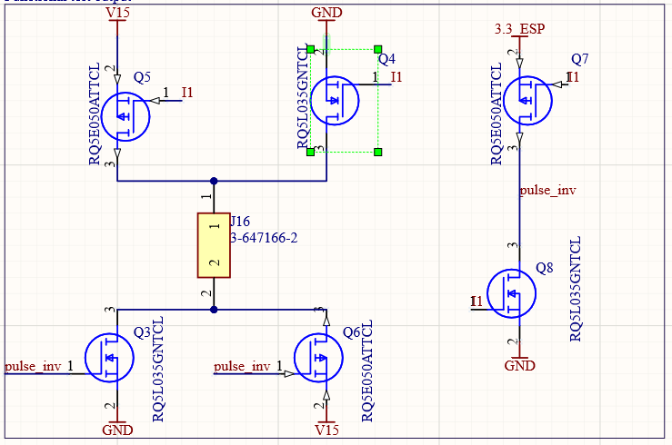
1653996555605.png
 

Hi,

a MOSFET is controlled by the voltage between it´s Gate and Source. Thus it´s name is V_GS.
--> Use a scope or voltmeter to measure V_GS of each MOSFET and find out if it´s ON or OFF.
To clarify: Not the voltage of Gate with respect to GND is what you have to care for.

I guess this is the problem.
I need to guess, because we have no information about the levels of "I1" and "pulse_inv"...also frequency, duty cycle, rise/fall rate...


Klaus


Hi klaus. Thanks for your fast reply.

I1 and pulse_inv are 3.3 constant signals.


If i eliminate q4 and q6 i have an 15V on/off circuit that works correctly ( I1=0, current through the load, I1=3.3V no current)... the problem is adding q3 and q5....

I also simulated this circuit and everything seems to work on the simulation ( with different transistors, because i didnt have the models )

1654004002270.png
 
Last edited:

Hi,

you have to bring the gate voltage of your p-channel MOSFET up to its applied source voltage, here 15 V. Otherwise, the gate-source voltage is not equal zero, and the P-MOSFET is still conductive when enabling the N-MOSFET. You are trying to control the P-MOSFET with a gate voltage of 3.3 V. As @KlausST mentioned, the voltage between gate and source matters.

BR
I guess this will solve the problem. Wjat do you guys think?

1654012197193.png
 

Hi,

Why don´t you draw the half bridges like every one else does?
It makes reading the schematic really hard.

Generally one tries to draw schematics
* with signal flow: left to right
* with the highest (supply) voltage (pointing) at top of page and lowest (supply) voltages (pointing) at bottom of page.

***
To your schematic:
It has some issues:
* low side drive level is 3.3V only ... maybe too low for saturated ON
* low side drive current unknown, maybe leads to slow turn ON and turn OFF
* high side drive level depends on bus voltage. Low bus voltage results in not clean switch ON, too high voltage (peaks) may distroy the gate
* high side drive current is very low, leading to very slow turn ON
* no clean dead time

So your circuit may work ....at a particular bus voltage and at low control frequency.....there is a big risk of fail with different conditions.

That´s why dedicated MOSFET drivers are available.

Klaus
 
Last edited:

Hi,

Why don´t you draw the half bridges like every one else does?
It makes reading the schematic really hard.

Generally one tries to draw schematics
* with signal flow: left to right
* with the highest (supply) voltage (pointing) at top of page and lowest (supply) voltages (pointing) at bottom of page.

***
To your schematic:
It has some issues:
* low side drive level is 3.3V only ... maybe too low for saturated ON
* low side drive current unknown, maybe leads to slow turn ON and turn OFF
* high side drive level depends on bus voltage. Low bus voltage results in not clean switch ON, too high voltage (peaks) may distroy the gate
* high side drive current is very low, leading to very slow turn ON
* no clean dead time

So your circuit may work ....at a particular bus voltage and at low control frequency.....there is a big risk of fail with different conditions.

That´s why dedicated MOSFET drivers are available.

Klaus
Thank you Klaus. I am learning a lot from you, thanks for that.

I clean a little bit the design as you recommend me to do:

1654171645503.png


This is a dc application, switch once per hour....

Some last questions:
* What do you recommend me to control the gate drive current of low side, high side and the other 2 extra mosfets ?
* My bus voltage comes from a dcdc with a 22uF out cap.. i think this can filter quite good the spikes right ?
Do you recommend me to place an extra capacitor in the gates that depend on the bus voltage ?


I am not an expert in power electronics, so this helps me a lot.
Thanks a lot again!
 
Last edited:

Hi,

Regarding schematic layout, I'd turn Q9 and Q10 around 180° and place them lower than the PMOS they drive. e.g. ground would be where ground is expected (bottom of schematic), instead of upside down and next to where only the V+ symbols are usually placed. At first sight, your NMOS just look like two more PMOS, that's not so helpful for someone to get a quick idea of the circuit.

- Resistors, maybe a Zener if gate voltages can exceed Vgs(max). If you mean a gate driver IC, no idea but there are plenty out there, people seem to use two a lot (sorry, don't know names, SGxxxx or UCxxxxx or something-or-other or something like that), so it would be wise to start with one of those in case you want to refer to application notes, design notes and forum threads whilst learning to use them. L293D is a basic bridge driver IC everyone knows, and very, very old.
- You'd need to know how solid your DCDC supply is, and from the load current (drawn once an hour), calculate if the 22uF capacitor can hold up the supply voltage for the time needed.
- Why on the gates? And potentially slow down turn-on and turn-off of the MOSFETs? I think your third question also relates to the correctly sizing the reservoir capacitors on the supply line, perhaps.

Gate driver ICs remove a lot of the problems you make for yourself with discrete designs, like dealing with dead-time/shoot-through, level-shifting (if needed).
 

Hi,

for your low switching frequency
* the usual "bootstrap" gate drivers are not useful
* maybe the photovoltaic gate drivers are the better choice.

Klaus
 

I will take a look at the Dcdc stability.
About the gate driving. I am using an esp32 directly to control the I1 gates... And then the inversor you see in the schematic to control the pulse_inv gates (3.3ESP comes from a 2A lado)


What do you think ?
 

You might include a series R between gate and ESP32 to limit max current dumped into
ESP32 power rails. That can affect its operation. Especially if you have several outputs
togging at once.

ESP32 may have a spec on max current allowed. Most modern micros have ports
with their own individual power rails, and limits total of what the rail can carry.

The sim is 0 ohms and 100 ohms for R1.

1654209760415.png


Regards, Dana.
 

Hi,

again: 3.3V (which is idealistically high) gate drive level is rather low. You can not expect the MOSFET to be fully ON.

Klaus
 

Hi,

again: 3.3V (which is idealistically high) gate drive level is rather low. You can not expect the MOSFET to be fully ON.

Klaus

Hi Klauss. By now it is working.

RQ5L035GNTCL VthGS= 1.3V -> teh conditions in my circuit will be 3.3V
RQ5E050ATTCL VthGS= -1:-2.5V -> the conditions in my circuit will be 0V or -15V
 

Hi,
RQ5L035GNTCL VthGS= 1.3V -> teh conditions in my circuit will be 3.3V
You are free to do so. But I call it "non reliable" design, because 1.3V is "best case" and only for 50uA of load current.

Datasheet says "worst case" V_gs_th for 50uA load current is 2.7V.

If it works for you it´s more "out of luck" .. but don´t be surprised if it fails. (getting hot, burn, catch fire, refuse to operate)

****
Additionally I think you have 3.3V as supply voltage, thus the pin output voltage always will be less.

Klaus
 

Hi,

You are free to do so. But I call it "non reliable" design, because 1.3V is "best case" and only for 50uA of load current.

Datasheet says "worst case" V_gs_th for 50uA load current is 2.7V.

If it works for you it´s more "out of luck" .. but don´t be surprised if it fails. (getting hot, burn, catch fire, refuse to operate)

****
Additionally I think you have 3.3V as supply voltage, thus the pin output voltage always will be less.

Klaus
In the circuit i have another 5V source... do you think is better to use it ? but for that i will need to include more mosfets in order to pass from the controll signal of 3.3V to 5V.. and i will have the same problem controling a gate with 3.3V... what do you recommend me to do ?
Thanks Klauss!
 

Status
Not open for further replies.

Part and Inventory Search

Welcome to EDABoard.com

Sponsor

Back
Top