Continue to Site

Welcome to EDAboard.com

Welcome to our site! EDAboard.com is an international Electronics Discussion Forum focused on EDA software, circuits, schematics, books, theory, papers, asic, pld, 8051, DSP, Network, RF, Analog Design, PCB, Service Manuals... and a whole lot more! To participate you need to register. Registration is free. Click here to register now.

MOS square low equation and inversion region

Status
Not open for further replies.

Junus2012

Advanced Member level 5
Joined
Jan 9, 2012
Messages
1,552
Helped
47
Reputation
98
Reaction score
53
Trophy points
1,328
Location
Italy
Activity points
15,235
Dear friends,

The square low equations are very useful approximation but only applied to the strong inversion and not in advance short channel technology,

All the literature books, like Allen Holberg, Paul Gray, Behzad Rezavi, etc, are consedring the strong inversion in the design with VDS(sat) around 100 mV or more,

Until I start to read the books of David Benkley and Paul Jespers , ("Tradeoffs and Optimization in Analog CMOS Design" and "Systematic Design of analog CMOS Circuits),

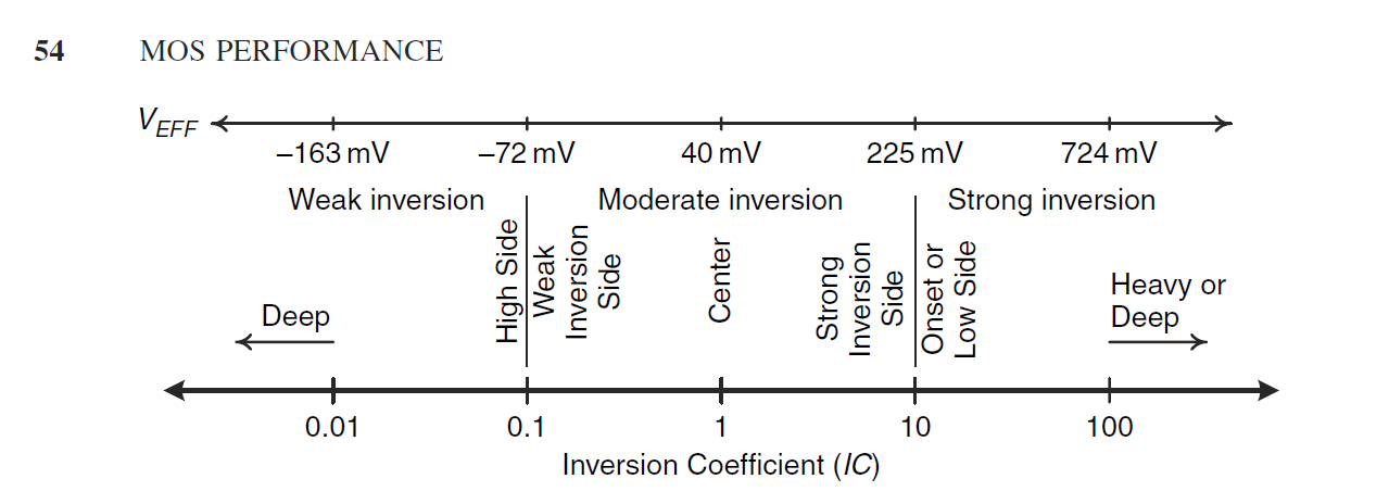
The latter authors both assumes that minumum VDS(sat) for saturation voltage is above 200 mV as you kindly see from this image
inversion.PNG


So my question, how the other books using the square low equations and they are not in the strong inversion, are they just approximating the solution as the 100 mV is at the border of strong inversion?

Bytheway, Gray stated that MOS enter the weak inversion if VDS(sat) is below 80 mV, which is quite different from the values given up

Thank you
Best Regards
 

Hi Janus,

First of all, congratulations for your new reading, I absolutelly love Binkley's book.

Bytheway, Gray stated that MOS enter the weak inversion if VDS(sat) is below 80 mV, which is quite different from the values given up

In this case, I believe Gray is refers to the center of the moderate inversion - as he was considering a "corner" between strong and week inversion, disregarding the moderate inversion region. We can do this calculation from the equation below:

\[ g_m(W.I.)=g_m(S.I.) \therefore \frac{I_d}{nV_T}=\frac{2I_D}{V_{gs}-V_{th}} \therefore V_{gs}-V_{th}=2nV_T \]

Using this value, we can get a very good approximation of the inversion coefficient.

I hope my answer can help you in some way.

Best regards!
Vitor
--- Updated ---

So my question, how the other books using the square low equations and they are not in the strong inversion, are they just approximating the solution as the 100 mV is at the border of strong inversion?

Regarding it, and also regarding Gray's book, a good approximation of Vdsat for moderate and week inversion is between 3 and 4 Vt, what is something between 77 and 100mV at room temperature.

Best regards
 
Last edited:
Thank you dear friend for your kind answer, it looks like VDSsat of 100 mV can be well treated or approximated using the strong region equations
 

Hi Junus,

Personally, I have the a conservative behavior in what concerns to the limit of \(V_{dsat} \) for strong inversion, since the main property that describes this operation region is the motion of carriers by drift as the main phenomenon (or, if you are more rigorous, as the absolute dominant phenomenon of carriers motion for really strong inversion).

Said that, considering a theoretical limiting as \( V_{dsat} \approx \frac{V_{GS}-V{th}}{n} \), I don't feel really confortable in considering any value below, let's say, 150mV of \(V_{dsat} \) if I really needs to ensure that my device is in strong inversion.

Anyway, if I have enough time, I really prefer to use the IC method of evaluation for a more criterious analysis.

If you have any different thoughts or interpretation regarding this, please let me know. I would be glad to have the opportunity to learn from someone's else experience :).

Kind regards,
Vitor
 
Hi Dominik,

I don't know if you were referring to my comments. I'm aware about the difference between those two quantities, but maybe some misunderstanding may be occurred from what I said.

Since Janus mentioned \( V_{d,sat} \) as his parameter of interest, I kept the analysis of this parameter instead of \( V_{od} \).

Nevertheless, as I said for Janus, if you have another interpretation or disagreement regarding my comments, please let me know. I'll also be glad to have the opportunity to learn from you :) .

Thank you and regards,
Vitor
 
Dear firends,

in long channel, overdrive voltage (Vov) is assumed as the minimum voltage of VDS saturation = (2Id/K' W/L)pow0.5.... which represent the edge of saturation,

However, for example in wide swing mirror, we bias the cascoded transistor above the edge of saturation to ensure safe region from the triode region, in this case I can say VDS(sat) > VoV

Dear sleepless, I use to follow Jakop procedure, in which for general design he use Vov = 5% VDD, in this case, with VDD = 3.3, then Vov = 165 mv, if Jakob is happy with this value I will also be happy, only concern in the book image I showed it looks like not in the strong inversion, hence square low equations is not very accurate to apply,

Argument done by some people, they say this value fall in to the high medium inversion, so by using square low equations it still good approxiamations, and by any way one must tune by simulation.
 
Hi Janus,

Thank you very much for sharing your design perspective.

In fact, if I'm not wrong, Binkley's considerations regarding \( V_{ov} \) for strong inversion are pretty similar to what is considered in EKV modelling. As I said, it considers as strong inversion the region which the carriers motion by drift phenomenon is absolutelly great than the motion by diffusion.

only concern in the book image I showed it looks like not in the strong inversion, hence square low equations is not very accurate to apply,

Regarding your comment, I believe that it is good to keep in mind that this image shown an approximation for a given technology/process (in this case, 0.18um I think). Since IC is defined according to the technology current, this 225mV of \( V_{eff} \) is not a constant value, but a technology dependent parameter.

Last (but not least), as you said, the range \[ 1\lt IC \lt 10 \] is also called moderate to strong inversion and this strong inversion approach may gives a good approximation and is also what I consider for my first calculations.

Kind regards,

Vitor
 
Regarding your comment, I believe that it is good to keep in mind that this image shown an approximation for a given technology/process (in this case, 0.18um I think). Since IC is defined according to the technology current, this 225mV of VeffVeff V_{eff} is not a constant value, but a technology dependent parameter.

Dear Sleepless

Thank you for your reply

How it is possible that Voff = 200 mV is a technology-dependent value ?
 

Janus,

Considering the below equation as a good approximation for the technology current, which defines the IC normalization:

\[ I_0\approx2n\mu_0C_{ox}V_T^2 \]

The substrate factor n, \[\mu_0\] and \[C_{ox}\] are technology dependents.

Considering the approximation for the \( V_{eff} \) at the center of the moderate inversion I described in my first post, you can see that even this value is technology dependent, since it is also a function of the substract factor. You can find some examples of variation according to technology in Tables 3.1 and 3.2 of Binkley's book.

I hope my reply can help you.

Kind regards,
Vitor
 
You can find some examples of variation according to technology in Tables 3.1 and 3.2 of Binkley's book.

Thank you dear for your reply, I have looked on those table but coudn't find Veff of other technologies
 

Hi Janus,

I reanalysed my assumptions and, taking a second look, the only technology parameter that really plays a role in \( V_{eff} \) for strong inversion is the substract factor. Find below my analysis.

Considering \( \frac{W}{L}=1 \)

\[ \frac{I_{D_{SI}}}{I_0}=10 \therefore I_{D_{SI}}=10I_0\therefore \frac{1}{2}\frac{\mu C_{ox}}{n}V_{eff}^2 \approx 20n\mu C_{ox}V_T^2 \therefore V_{eff}\approx nV_T\sqrt{40} \]

My apologies for the misleading information I gave you before. Please, let me know if you find any misconception in my analysis.

Kind regards,
Vitor
 
Just adding information, a more precise analysis is provided in Section 3.7.2 in Binkley's book.
 

I reanalysed my assumptions and, taking a second look, the only technology parameter that really plays a role in VeffVeff V_{eff} for strong inversion is the substract factor. Find below my analysis.

Dear Sleepless, n represent the substrate factor or the of the subthreshold slop factor ? how can I find this value of my used technology
 

Hi Junus,

n represent the substrate factor or the of the subthreshold slop factor ? how can I find this value of my used technology

Per my understanding, the subthreshold slope factor is a function of the substrate factor, given by the equation below:

\[ S\approx n\frac{kT}{q}\ln(10) \]

The substrate factor is given by the inverse of the capacitive division between the gate and the substract. It can be extracted from the following relation between \( g_m \) and \( g_{mb} \):

\[ n = 1+\frac{C_{dep}}{C_{ox}}=1+\frac{g_{mb}}{g_m} \]

Normally it is a value between 1.2 and 1.5.

Kind regards,
Vitor
 

    Junus2012

    Points: 2
    Helpful Answer Positive Rating
You're very welcome my friend.

The typical value is between 1<n<3

For submicrometer technologies, I usually found values between 1.2 and 1.5 (I believe that Sansen and/or Binkley also reports this range in literature).

s affordable by process information or need to be extracted?

You can refers to the section 3.4.1 of Binkley's book for detailed information. This value varies slightly with gate-source voltage, and hugely with source-bulk voltage (figure pasted below, for your convenience).

1602855249268.png

Figure 1 - Predicted substrate factor, n, versus gate–source voltage with overlay of measured 1+gmb/gm for nMOS devices in a 0.18\(\mu\)m CMOS process (copied from BINKLEY, Tradeoffs and optimization in analog CMOS design).


My opinion is that is better to "extract" it from PDK from the aforementioned OP parameters (\( g_m \) and \( g_{mb} \)).

Kind regards,
Vitor
 
Thank you dear friend for your kind and helpful answer
 

Status
Not open for further replies.

Part and Inventory Search

Welcome to EDABoard.com

Sponsor

Back
Top