Continue to Site

Welcome to EDAboard.com

Welcome to our site! EDAboard.com is an international Electronics Discussion Forum focused on EDA software, circuits, schematics, books, theory, papers, asic, pld, 8051, DSP, Network, RF, Analog Design, PCB, Service Manuals... and a whole lot more! To participate you need to register. Registration is free. Click here to register now.

Measuring DC voltage outside ADC range

Status
Not open for further replies.

Eight

Member level 2
Joined
Mar 8, 2013
Messages
53
Helped
1
Reputation
2
Reaction score
1
Trophy points
1,288
Activity points
2,084
Hello.

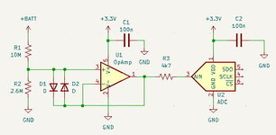
I'm designing a circuit to measure DC voltages that can be higher than what the ADC can handle. I already did some searching/googling, but I'd like to ask someone to verify, if what I'm doing is correct. The measured voltage span should be from 0 to 16V DC, and I only need continuous low-speed measurements of DC (battery voltage).

Obviously, I will need a two-resistor voltage divider to bring the measured voltage down to acceptable levels (the single-ended ADC can only go up to 3.3V). The first question is how high resistor values to use. Most ADC's require some maximum source impedance for accurate measurements (usually up to 10 kOhm). But since this is going to be a battery powered application I would like to minimize the current flow through this voltage divider - this means resistor values should be in range of some megaohms. Unfortunately those values will result in a current that is insufficient for the ADC. Therefore, the source should be buffered by an opamp in a unity-gain voltage follower configuration. Finally, I'd like to add some overvoltage protection to the opamp input as a good measure.

Attached is the circuit that I came up with.
I'm not sure what type of diodes to use except that they should be low-leakage (someone suggested junction diode?).
Any other thoughts, suggestions?

Thanks in advance!
 

Attachments

  • adc.jpg
    adc.jpg
    21.9 KB · Views: 161

The reason for needing low(ish) impedance at the input of an ADC is that internally most MCUs have to draw a small input current to charge their sampling circuit at the start of a measurement. If the values are too high, that current causes a drop in measurable voltage. As the frequency of measurement speeds up, the need to give time for the voltage to recover becomes longer. In your application where the measuring is low speed you can overcome the problem by simply adding a capacitor across the ADC input. It will keep the voltage stable for the duration of the measurement.

For protection, I would suggest two small-signal Schottky diodes, one from the input to ground, one from the input to 3.3V, both 'cathode up" so they are normally not conducting. Any negative voltage will be clamped by the ground side diode and anything higher than supply will be clamped by the other one. Schottky diodes have a lower Vf than the inputs of most ICs so they will conduct most if not all dangerous currents away from the ADC pin.

Brian.
 

High valued R thermal noise can contribute to error, for apps using
delsig types of converters operating 20 bits or greater.....in general

1669041248141.png


What is the resolution of the ADC you are working with ?

Typically datasheet shows input sampling structure and its parasitics.
Refer to that for guidance.

Using an OpAmp, in this case you probably need a RRIO type, input
stages exhibit crossover distortion, so beware of that. Some datasheets
discuss this, some do not.

Of course the OpAmp contributes errors. You should do an end to
end error budget analysis to see if you meet your goals.


Regards, Dana.
 

Hi
Change the ratio of R1&R2 for voltage in scale of ADC.
Reduce R3 < 1k Ohm, and add Ca Capacitor for pin3 of ADC. R3 & C3 creat a LPF, which design for filter noise and cut off frequency higher than sample frequency of ADC. R3 too high will make drop voltage on it when has charge current input of ADC. If high speed ADC will absorb more current. This make error to measured result.
If Opam is low power type, check it is rail to rail type or not, that mean how much span output voltage you can use. Example, normal opam output only maximum is Vcc - 1.5V, rail-to-tail type accept Vcc - 0.6V.
Because of input high impedance source mega ohm, check input offset current of opam, that will make error for resistor devider, also make error for linear ratio.
As I suggest, I don't use this solution to save power when measure Vbat. I use a switch to turn on connection to Vbat when I want to measure. This time circuit will asorb current. After measure, turn off, then no current discharge from battery. This solution can save more power, and accept lower resistor devider for lower linear error, low cost opam can use.
 

For protection, I would suggest two small-signal Schottky diodes
Are you sure about the Schottky diodes? I've seen some circuits that are exactly what you're proposing, but I've also read on several pages that those diodes are very leaky and can impact the measurement significantly. They have a reverse current of several tens or even hundreds of uA compared to a junction diode that is just a few nA.

What is the resolution of the ADC you are working with ?
The ADC is 12-bit SAR. I don't think resistor noise is going to be a problem though, but thanks for pointing it out.
Yes, ideally the opamp should be R2R.

Reduce R3 < 1k Ohm, and add Ca Capacitor for pin3 of ADC.
The ADC datasheet says its source impedance must be max 10kOhm, so I think a 4k7 resistor should be fine. Though I could add an extra cap there for good measure.

I use a switch to turn on connection to Vbat when I want to measure. This time circuit will asorb current. After measure, turn off, then no current discharge from battery. This solution can save more power, and accept lower resistor devider for lower linear error, low cost opam can use.
Yeah, I've been thinking of adding a switch and only enable the circuit during measurements. What king of switch do you propose? I take it a low-side N-MOS is a no-no, so perhaps a high-side P-N complementary pair?

Regards!
 

Are you sure about the Schottky diodes? I've seen some circuits that are exactly what you're proposing, but I've also read on several pages that those diodes are very leaky and can impact the measurement significantly. They have a reverse current of several tens or even hundreds of uA compared to a junction diode that is just a few nA.
Schottky diodes are indeed more leaky in reverse direction but the amount is insignificant for your application. If you look at the data sheet for the BAT85 for example, it quotes 2uA maximum at 25V but the graphs of Vr and Ir show that 3.3V it goes off the scale at somewhere below 100nA.

Brian.
 

I see. So, how does the diode layout that you proposed (one "cathode up" diode from Vcc to IN+ and another from IN+ to GND) compare to the one I posted in my first post (two diodes in a diac-like configuration from IN+ to opamp output)?
 

Hi,

Diodes to IN+:
+ can be expected to cause zero leakage (no glas package), because there is about zero voltage between IN+ and IN- during normal operation
- pass all the current to the OPAMP output. Thus the protection relies on the Opamp output strength
- provide about no protection when Opamp is powered OFF.

I'd use a high ohmic voltage divider. Or a lower phmic dividervand a P-Ch Mosfet as high side switch.
Also I'd use a storage capacitor to compensate the high ohmic source.

It all depends on the expected accuracy and the ADC input characteristics (mainly input current and input capacitance)
If you need 1% accuracy,
* then the external capacitor needs to be 100x the ADC input capacitor.
* then the switch needs to be ON at least 4 tau before the conversion starts.

Klaus
 

I see. So, how does the diode layout that you proposed (one "cathode up" diode from Vcc to IN+ and another from IN+ to GND) compare to the one I posted in my first post (two diodes in a diac-like configuration from IN+ to opamp output)?
I wouldn't think of that as a 'diac-like' configuration, as anti-parallel diodes do not exhibit the avalanche characteristics of a real diac.

The problem with your connection is you are still prone to excess voltage damaging the IC. Although it sinks/sources current from the op-amp output to counter any excess input voltage, it still only works within the supply range of the IC and possibly in one polarity. The diode to ground and diode to 3.3V does introduce a tiny measurement error but it should be insignificant especially as you are only measuring battery voltage, however it greatly increases the degree of protection against over voltage and reverse voltage at the input.

If you are only expecting brief transient over-voltages, the capacitor alone should suffice.

If you really need extreme low current consumption from the battery, consider a very high value feed resistor and a low-leakage transistor to ground, driven from your MCU. Use it to clamp the voltage across the capacitor to (almost) ground. When the transistor is turned off, take two measurements from the ADC and calculate the battery voltage from the rate of voltage rise. Knowing the tau you can make sure the transistor is turned back on again before the voltage can rise too high to cause damage.

Brian.
 

Hmm, all good points. Alright, thanks for the information. I think I have enough knowledge now to start building some circuits. I'll do some measurements to see the linearity.

Best regards!
-E
 

I'll do some measurements to see the linearity.
I don´t expect linearity issues caused by the external circuit. I´d rather expect gain and offset errors.

Klaus
 

Status
Not open for further replies.

Similar threads

Part and Inventory Search

Welcome to EDABoard.com

Sponsor

Back
Top