Continue to Site

Welcome to EDAboard.com

Welcome to our site! EDAboard.com is an international Electronics Discussion Forum focused on EDA software, circuits, schematics, books, theory, papers, asic, pld, 8051, DSP, Network, RF, Analog Design, PCB, Service Manuals... and a whole lot more! To participate you need to register. Registration is free. Click here to register now.

MC145151 for only 457KHz and 453KHz Switches position?

Status
Not open for further replies.

neazoi

Advanced Member level 6
Joined
Jan 5, 2008
Messages
4,123
Helped
13
Reputation
26
Reaction score
15
Trophy points
1,318
Location
Greece
Activity points
36,955
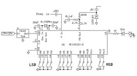
Please help me set this PLL switches for
A: 457KHz
B: 453KHz
Which switches do I need to close?

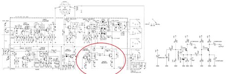
This is to be applied to the BFO of the FRG-7 receiver shown. Any thoughts where to connect the varicap to vary the frequency of the BFO with the minimum mods to the radio, will be appreciated.
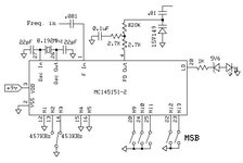
 

Attachments

  • unipll1_simplistic_version.jpg
    unipll1_simplistic_version.jpg
    32.5 KB · Views: 238
  • my_frg-9_mods1.jpg
    my_frg-9_mods1.jpg
    428 KB · Views: 194

RA0,RA1,RA2 should be 0 for 1kHz Frequency Step. ( Pin No 5,6,7 respectively)
N Counter should be programmed as Fin/Fref
So N will be between 453 and 457 and it must be programmed as binary codes.

This is for MC145151-2 Single Modulus PLL. Programmation fo 145152-2 is different.
 
Last edited:

    neazoi

    Points: 2
    Helpful Answer Positive Rating
RA0,RA1,RA2 should be 0 for 1kHz Frequency Step. ( Pin No 5,6,7 respectively)
N Counter should be programmed as Fin/Fref
So N will be between 453 and 457 and it must be programmed as binary codes.

This is for MC145151-2 Single Modulus PLL. Programmation fo 145152-2 is different.
Thank you very much, but would that be easy for you to suggest me the actual pin numbers for the 2 frequencies of interest, just to avoid any confusion or mistakes?
 

It is just the binary representation of the divisor so for 453 it is 111000101 with the last digit being N0 and for 457 it is 111001001 so you only have to change N2 and N3 to switch frequencies, the rest can be hard wired.

Use the varicap circuit in the first picture with the series capacitor across C436, if you don't get enough frequency shift, connect it to the drain of the FET instead. Extract the input frequency (F in) from the emitter of Q409. You might have to slightly retune T406 to compensate for the extra capacitance across the tuned circuit.

Brian.
 

    neazoi

    Points: 2
    Helpful Answer Positive Rating
Hi,
Thank you very much, but would that be easy for you to suggest me the actual pin numbers for the 2 frequencies of interest, just to avoid any confusion or mistakes?
I solved it using an internet search: "decimal binary converter online"
example: input decimal value 457 to get the binary representation.

Klaus
 

It is just the binary representation of the divisor so for 453 it is 111000101 with the last digit being N0 and for 457 it is 111001001 so you only have to change N2 and N3 to switch frequencies, the rest can be hard wired.

Use the varicap circuit in the first picture with the series capacitor across C436, if you don't get enough frequency shift, connect it to the drain of the FET instead. Extract the input frequency (F in) from the emitter of Q409. You might have to slightly retune T406 to compensate for the extra capacitance across the tuned circuit.

Brian.
Like this?
How about N9 to N13? Do they need to be open or closed?
Also how about ra0,ra1,ra2, do they need to be all open (since I am using the 8.192MHz crystal and I need 1KHz step)?
 

Attachments

  • 455.jpg
    455.jpg
    24.4 KB · Views: 105
Last edited:

All the RA and N pins have internal pull-up so you can leave all the RA pins unconnected to get the 1KHz divider reference. For the N pins, you have to put the exact binary number across all the pins so the 'unused' most significant bits will have to be grounded, only the ones with a '1' in the number must be high.

Brian.
 

    neazoi

    Points: 2
    Helpful Answer Positive Rating
All the RA and N pins have internal pull-up so you can leave all the RA pins unconnected to get the 1KHz divider reference. For the N pins, you have to put the exact binary number across all the pins so the 'unused' most significant bits will have to be grounded, only the ones with a '1' in the number must be high.

Brian.
This is wrong. R Counter should be programmed as R0=0 R1=0 R2=0 so these pins must be pulled down by force.
N Counter "zeros" must also be pulled down by force by connecting to GND.
 

According to the data sheet if all 'R' pins are zero, the reference divider is 8. When they are all high it is 8192.

The desired reference is 1KHz and the crystal is 8192KHz so 8192 is the correct divisor to use.

Brian.
 

Hi,

the mistake lies in post#2:
"RA0,RA1,RA2 should be 0 for 1kHz Frequency Step."

it should be:
"RA0,RA1,RA2 should be 1 for 1kHz Frequency Step."

so 8192 kHz in --> divided by 8192 --> 1kHZ
RA0, RA1, RA2 left open is correct.

Klaus
 

You are both right. This is my mistake..
R0=R1=R2=0 and N Divider will have 453-457 whatever is..
 

Status
Not open for further replies.

Part and Inventory Search

Welcome to EDABoard.com

Sponsor

Back
Top