Continue to Site

Welcome to EDAboard.com

Welcome to our site! EDAboard.com is an international Electronics Discussion Forum focused on EDA software, circuits, schematics, books, theory, papers, asic, pld, 8051, DSP, Network, RF, Analog Design, PCB, Service Manuals... and a whole lot more! To participate you need to register. Registration is free. Click here to register now.

matching AD8277 spice symbol with data sheet

yefj

Advanced Member level 4
Joined
Sep 12, 2019
Messages
1,196
Helped
1
Reputation
2
Reaction score
3
Trophy points
38
Activity points
7,223
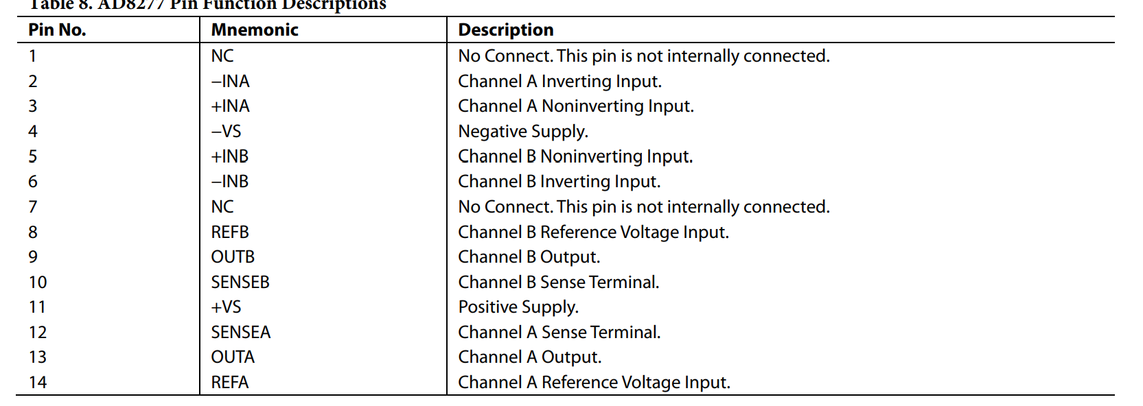
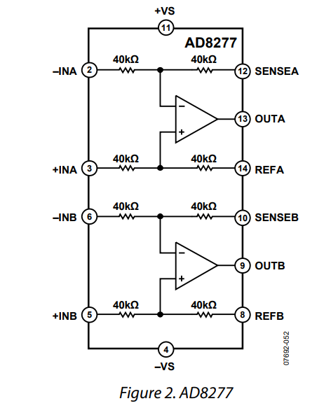
Hello,given the datashhet below. it have many pins
the ltspice model is attached in the link.
all pins are attached in the table bellow.
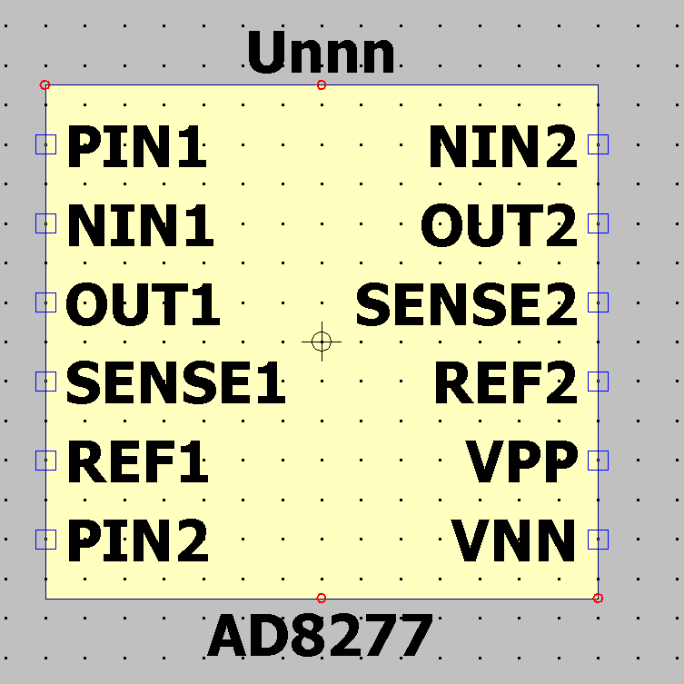
when i created the ltspice simbol it gives me NIN1,PIN1 VNN as shown below.
How do i know what these names of the symbol represent in the datasheet?
Thanks.
1695063831187.png
1695066020287.png
1695065815823.png
 
Hi,

PINx should be the positive input of opmap x (1 or 2) and NINx the negative one. VPP the positve supply and VNN the negative supply.

Usually a detailed look in the Spice file provides the information, see below. Here the pin order is important.

Screenshot_20230918-222805~2.png


BR
 
Last edited:
Hi,

this depends on your application. I would recommend to have a detailed look in the Application Information section.

1. what is the difference between sensing output and normal output?

The Sense Terminal grants excess to the internal resistor, which is matched with the other internal resistors, consequently minimizing errors, see below. So depending on your aimed circuit function, you may directly connect this SENSE pin wit the output OR somewehre else where e.g. see Figure 50.

1695149652697.png


2.what is the reference voltage is use for?
For example you can connect the REF pin to GND or to a voltage (provided by a low impedance source) for level shifting purpose.

3. given the datasheet below how do i know what voltage range the device is supposed to be recieving?
From the front page:
1695149892966.png


... keeping the absolut maximum ratings in mind.
1695149954076.png


BR
 
Hello, i have tried to simulate this device as shown below.
Its supposed to be unity gain device, so when i input 3V its supposed to give me 3V on the output.
Instead i get 15V.
Where did i go wrong connecting this device?
Thanks.
1695150475390.png
 
Please have a look in the dataseet. Than have a look how a unity gain amplifier (buffer) is realized with an opamp.

What you have wired up so far is the following...

1695151540479.png


... that simply can not work.

BTW, you can freely modify the LTSPICE symbol so it looks like the one in the datasheet, to avoid any confusion.

BR
 
Hello, from the diagram below we have GND at the minus and Vin/2 at the plus (40K 40K voltage divider).
so i am supposed to get Vin/2 at the output.(buffer)
Where my logic is wrong?
Thanks.

1695153120741.png
 
... the SENSE pin is open, so the opamp has no feedback. Keep in mind, the opamp tries to keep the voltage difference between its input as close ase possible to 0 V. No feedback, no regulation.

Have you actually checked how an unity amplifier is wired up?
 
... the SENSE pin is open, so the opamp has no feedback. Keep in mind, the opamp tries to keep the voltage difference between its input as close ase possible to 0 V. No feedback, no regulation.

Have you actually checked how an unity amplifier is wired up?
Hello, if Sense is open then the whole node is GND and gnd goes to minus.
so the buffer will be 1*(Vplus-Vminus)=1*(Vplus-0)
its straight forward amplifier logic,it doesnt need a feedback.
why my logic is wrong?
 
Sorry, but simply NO.

How should the opamp regulate ist output? I would highly recommend to have a look in a textbook and refresh some basics. What you have wired up, is a comparator, thus resulting in the high voltage of ~15 V (see [1]).

[1] https://www.electronics-tutorials.ws/opamp/op-amp-comparator.html

See below the simple results, I used an abritrary opamp with a bipolar supply. And yes, due to the feedback you are getting as a result 3 V, as this configuration will result in a gain of 2.
1695154412966.png


1695154478817.png


BR
 
Yes you are abslolutly correct it is a comparator and we get an output of 15 or -15.
In opamps we have virtual ground property and V_ouput=A*V_input
So its not an OPAMP?
we dont have virtual pin connection property?
How do i analyze the feedback connection if we dont have virtual input pin connection property?
Thanks.
 
Virtual ground is a concept commonly used with inverting amplifiers, so you can wire up the AD8277 as inverting opamp connecting the +IN and REF pin to system ground. Consequently, you have ~0 V at the posetive input ( ~0 V because of the input bias currents and the 40k || 40k --> 20k resistor towards GND). In an inverting feedback configuration (here you would have a gain of -1, when using the inrenal 40k resistors), the opamp is trying to keep the voltage difference between its inputs (close) at 0 V. Now you can find your virtual ground at the negative input of the opamp.

Please have a look in a textbook or webpages to refresh your opamp basics.

https://electrosome.com/virtual-ground-opamp/

BR
 
Hello Stenser , this opamp has unity gain(buffer) ,virtual ground assumes infinite gain -> thus V+=V-
I want to analize this configuration mathematickly.
What assumption do i make when analyzing feedbak of unity gain amplfier?
Thanks.
 
Hi,

in which kind of analyzation you are interested exactly? This should be a straight forward task. If you are strugling because you are mixing up closed-loop gain with open-loop gain, have a look here

https://www.analog.com/media/en/training-seminars/tutorials/MT-033.pdf

Please show what you have done so far and what is your aim/goal. This thread started with the pin assignment of a SPICE model and now we are talking about a mathematical analyzation, feels like an odyssey to me.

BR
 

LaTeX Commands Quick-Menu:

Similar threads

Part and Inventory Search

Welcome to EDABoard.com

Sponsor

Back
Top