Continue to Site

Welcome to EDAboard.com

Welcome to our site! EDAboard.com is an international Electronics Discussion Forum focused on EDA software, circuits, schematics, books, theory, papers, asic, pld, 8051, DSP, Network, RF, Analog Design, PCB, Service Manuals... and a whole lot more! To participate you need to register. Registration is free. Click here to register now.

LNA MIXER circuit help

Status
Not open for further replies.

areeb

Junior Member level 2
Joined
Jan 28, 2009
Messages
20
Helped
3
Reputation
6
Reaction score
3
Trophy points
1,283
Activity points
1,421
Hi Guys!

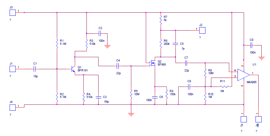
I am having problem figuring out a circuit (Attached in the message). I can identify the components individually but I cannot figure out what is the purpose of this circuit or where is it used. It looks like an fm transmitter/receiver/LNA/MIXER circuit, but I am not sure. Any suggestion would be of great help.
Thank you in advance!

Also please let me know the function of pins (I/O) ports shown with question marks on the figure.Thanks


Attachments

  • Untitled.png
    Untitled.png
    32.2 KB · Views: 97


As the MAX985 is a fast comparator with up to 1 GHz response, your circuit looks like a RF preamp followed by a mixer/comparator. If the LO input is fed from a swept-frequency oscillator, the comparator will generate a pulse every time the RF input signal gets close to the LO signal (twice each sweep).
Similar circuits are used in police-radar detectors, with RF down converters before them, that define the microwave range (S-band, C-band, Ku-band. etc.). Possibly also in UHF scanners to "catch" at a RF signal close to LO frequency.
 
  • Like
Reactions: areeb

    areeb

    Points: 2
    Helpful Answer Positive Rating
Hi, thank you for the reply, what i understood from your explanation is that there are 3 stages, the first stage is the pre-amplifier and the last is the high speed comparator, what about the middle stage? And what is the purpose of the pins J1 and J2? J3, J4, J5 seem to be the power rails of the circuit.
 

Hi, thank you for the reply, what i understood from your explanation is that there are 3 stages, the first stage is the pre-amplifier and the last is the high speed comparator, what about the middle stage? And what is the purpose of the pins J1 and J2? J3, J4, J5 seem to be the power rails of the circuit.

J1 is the RF signal input, J2 the LO input. The second RF stage may act as a limiter. As no filters are shown, I can only guess that the circuit can process VHF and UHF. If you have it, you can power it with +5 V to J3. My guess is the the J2 LO input may need a LO signal from a swept VCO, +10 dBm.
 
  • Like
Reactions: areeb

    areeb

    Points: 2
    Helpful Answer Positive Rating
The resistor values are much too high for the first transistor and Mosfet. Then the current in them is much too low for them to do anything.
 

Hi, thank you for replying, so what do you mean when you say the current is too low and it will not do anything? Like the input resistance of a MOSFET is R5->10Mohm to minimize the gate current. Isn't that fine? Similarly larger the input resistance of the BJT, larger the beta (B), the more ideal it will behave? Thanks in advance!
 

You do not say the supply voltage but the transistor and Mosfet have maximum voltages of 12V. Then if the supply is 10V and the transistor is biased so that there are equal 3.3V voltages across the collector resistor, the emitter resistor and transistor then its collector-emitter current is only 3.3V/510k= 6.5uA. Its datasheet has all its spec's listed when its collector-emitter current is 770 times higher (5mA).
The current gain of a transistor at very low currents like this one is extremely low.
 

Status
Not open for further replies.

Similar threads

Part and Inventory Search

Welcome to EDABoard.com

Sponsor

Back
Top