gvi70000
Member level 5
Hello all,
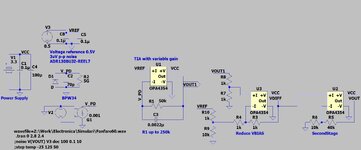
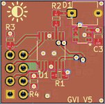
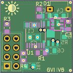
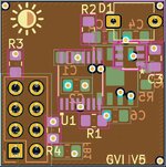
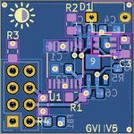
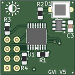
I need your help in checking the attached schematic before I will send the PCB to manufacturing.
The idea behind it is to have a variable sensitivity sensor that will feed the ASC of a microcontroller.
As sensitive element I am using a BPW34 PIN photodiode. The current generated is fed into a TIA that has a variable gain set by the digital pot.
For it to work when no current is flowing I have used a small voltage bias.
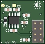
In the second stage I am removing the bias from the TIA output.
The third stage is again an amplifier to be able to amplify very weak signals.
The last stage is a buffer and I am using R12+C6 to smooth the output signal.
Please let me know your opinions, will the circuit work as described? Do you have any improvements to propose?
Thank you for your support,
Ion
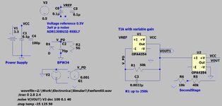
I need your help in checking the attached schematic before I will send the PCB to manufacturing.
The idea behind it is to have a variable sensitivity sensor that will feed the ASC of a microcontroller.
As sensitive element I am using a BPW34 PIN photodiode. The current generated is fed into a TIA that has a variable gain set by the digital pot.
For it to work when no current is flowing I have used a small voltage bias.
In the second stage I am removing the bias from the TIA output.
The third stage is again an amplifier to be able to amplify very weak signals.
The last stage is a buffer and I am using R12+C6 to smooth the output signal.
Please let me know your opinions, will the circuit work as described? Do you have any improvements to propose?
Thank you for your support,
Ion