Continue to Site

Welcome to EDAboard.com

Welcome to our site! EDAboard.com is an international Electronics Discussion Forum focused on EDA software, circuits, schematics, books, theory, papers, asic, pld, 8051, DSP, Network, RF, Analog Design, PCB, Service Manuals... and a whole lot more! To participate you need to register. Registration is free. Click here to register now.

[SOLVED] Kick-back noise of a latch comparator

Status
Not open for further replies.

canarybird33

Member level 1
Joined
Apr 16, 2013
Messages
41
Helped
2
Reputation
4
Reaction score
2
Trophy points
1,288
Location
Mashhad, Iran, Iran
Activity points
1,591
Hello all,
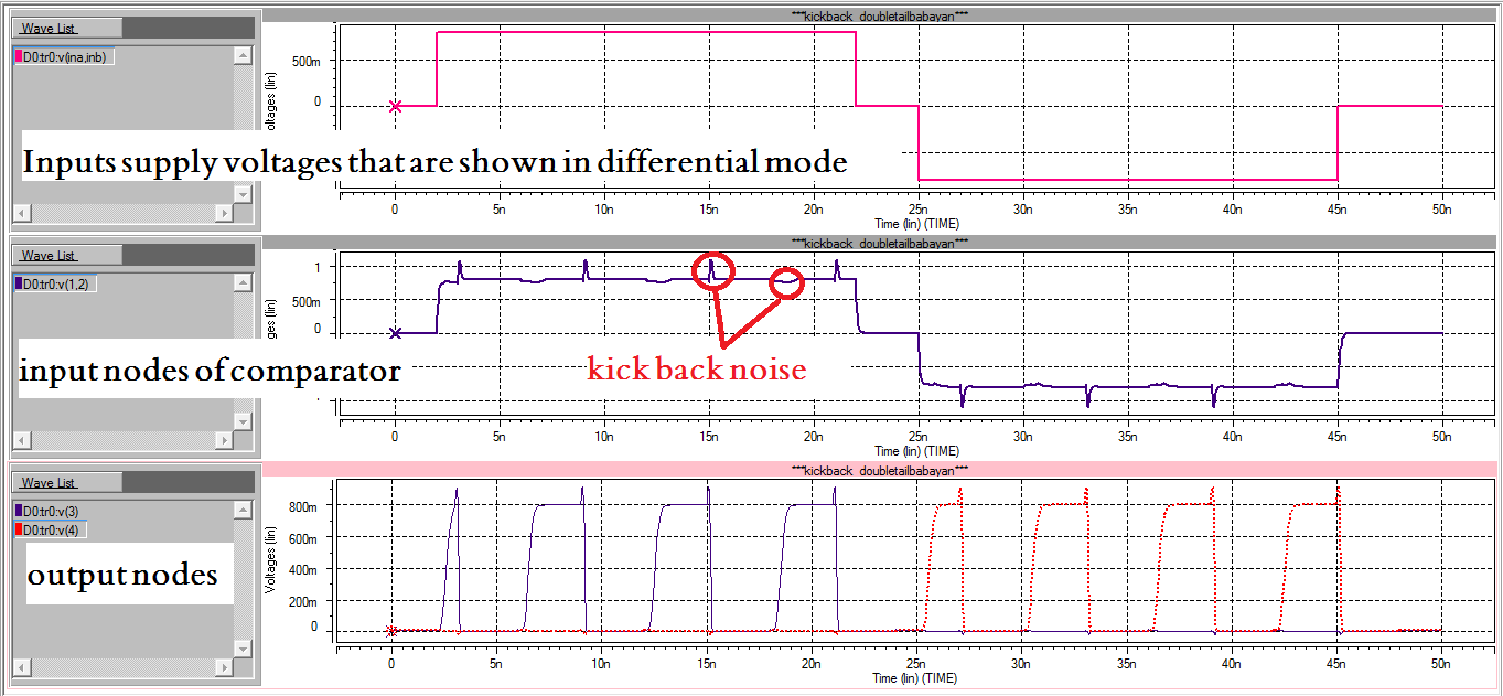
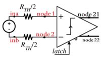
In my searches,the below method is used to calculate kickback noise.(Rth=8kohm; according to the this paper "Kickback Noise Reduction Techniques for CMOS Latched Comparators"]


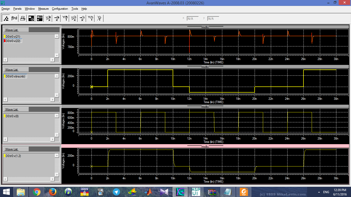
My simulation doesn't show sensible results. I mean, when I apply this method, the comparator does not work properly. the simulatin results are as follows (Node 21 and Node 22 are outputs):


My questions are:
should the comparator work as normal when calculating kickback noise?
Is the Rth=8kohm a general rule? Why 8k?
How should I apply the ina and inb as inputs?(I have applied 2 separate pulse to create the signal as same as the paper I mentioned above)
Thanks.
 
Last edited:

That circuit cartoon provides no common-mode authority for
the inputs. Where are they sitting "naturally" and is that
within the proper-function common mode range spec? If
this is a single supply comparator, does it work with both
inputs near ground (neg supply)? An NMOS-input design
would not, the input pair would be choked off.

It appears that the outputs are both pinned to an output
common mode reference (or arbitrary) point developing no
difference. That is one outcome of front end failure.

RTH should be the source impedance of what's driving
your comparator in the target application. 8K may match
what whoever made the figure, was looking at.

Kickback noise only matters when the comparator is
about its business and comparing signals closer-together
than the noise amplitude. So chicken/egg to some extent
but a comparator that's not comparing, who cares?
 
dick_freebird, thank you.
I applied a proper common mode voltage, so the comparator can compare right now.
I re-simulated the proposed circuit in paper "Analysis and Design of a Low-Voltage Low-Power Double-Tail Comparator". kick back noise has been reported 43 mv while in my simulation is more than 200mv in the falling edge of the clock.

both falling edge and rising edge are important?
 

The important noise is the noise that precedes the decision /
latch event. Much of it may be generated by the zero-ing
switch releasing, but some of it probably comes after the
decision has been made. So even though it may be quantitatively
large, the question is how much it affected the decision
(a Vio adder as it were).

At higher speeds the settling time from the previous kick
becomes interesting. Probably the kick that attends the
zero phase will get taken out (unless you're right up
against the performance limits of the design & process).

It appears that the "right answer" is resulting (at a gross
input overdrive). And the noise you are identifying looks
to be coming at the inactive phase where you go back
into nulling.

I would suggest incrementally reducing the input difference
and see what your zero-impedance Vio and your 8Kohm
input impedance Vio look like (the Zin=0 case would squash
any kickback, the 8K will turn it into a common mode
transient I'd expect, to be dealt with by transient / HF
CMRR). Get to less Vin than the design spec for sure,
because this is where kickback matters.
 
Status
Not open for further replies.

Part and Inventory Search

Welcome to EDABoard.com

Sponsor

Back
Top