Tukan
Junior Member level 1
Hello,
I am posting two pictures.

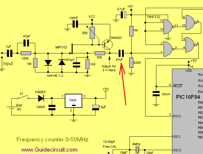
On Picture 1. is the JFET driving PNP BJT through voltage drop on R1 - this is common circuit how I found on internet by many similar variants.
On Picture 2. is the same JFET, but driving NPN BJT through voltage drop on R2 - I would rather use this variant because of presence NPN tranzistor, which is much more simple to obtain for high frequencies (I want measure up to 220 MHz) - but I am confused about using it because sources I read were describing only just driving BJT through R1 - on Drain side.
Can somebody give me opinion about Picture 2. , whether this circuit is usable please?
Thanks in advance.
I am posting two pictures.

On Picture 1. is the JFET driving PNP BJT through voltage drop on R1 - this is common circuit how I found on internet by many similar variants.
On Picture 2. is the same JFET, but driving NPN BJT through voltage drop on R2 - I would rather use this variant because of presence NPN tranzistor, which is much more simple to obtain for high frequencies (I want measure up to 220 MHz) - but I am confused about using it because sources I read were describing only just driving BJT through R1 - on Drain side.
Can somebody give me opinion about Picture 2. , whether this circuit is usable please?
Thanks in advance.